
PCB EMI Shielding: Techniques, Materials, and Best Practices
Introduction
Electromagnetic interference (EMI) is a significant challenge in modern electronics, affecting the performance and reliability of printed circuit boards (PCBs). As electronic devices become more compact and operate at higher frequencies, managing EMI becomes crucial to ensure signal integrity, compliance with regulatory standards, and optimal device functionality.
PCB EMI shielding involves techniques and materials designed to minimize unwanted electromagnetic radiation from electronic circuits. This article explores the fundamentals of EMI shielding, common shielding techniques, materials used, and best practices for effective EMI suppression in PCB design.
1. Understanding EMI in PCBs
1.1 What is EMI?
EMI refers to the disturbance generated by electromagnetic fields that interfere with the operation of electronic circuits. It can be classified into two types:
- Conducted EMI – Propagates through conductive paths like power lines or PCB traces.
- Radiated EMI – Travels through the air as electromagnetic waves.
1.2 Sources of EMI in PCBs
- High-speed digital signals (e.g., clock signals, data buses)
- Switching power supplies
- RF circuits (e.g., Wi-Fi, Bluetooth modules)
- Crosstalk between adjacent traces
- Poor grounding and return path design
1.3 Effects of EMI
- Signal degradation and data corruption
- Increased bit error rates in communication systems
- Failure to meet regulatory standards (e.g., FCC, CE)
- Malfunctioning of sensitive analog circuits

2. PCB EMI Shielding Techniques
Several techniques are employed to mitigate EMI in PCBs, categorized into layout strategies, shielding enclosures, and filtering methods.
2.1 PCB Layout Strategies
Proper PCB layout is the first line of defense against EMI. Key techniques include:
- Ground Planes – A solid ground plane reduces EMI by providing a low-impedance return path.
- Signal Routing – High-speed signals should be routed away from sensitive analog circuits.
- Differential Pair Routing – Minimizes radiated emissions by canceling out opposing currents.
- Controlled Impedance Traces – Ensures signal integrity and reduces reflections.
- Via Stitching – Placing multiple vias around high-frequency traces to contain EMI.
2.2 Shielding Enclosures
Metallic shields are commonly used to block radiated EMI. These include:
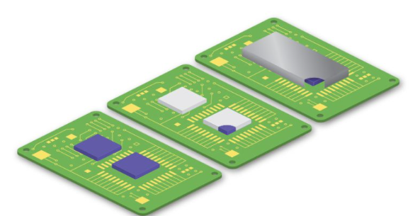
- Board-Level Shields (BLS) – Custom metal cans soldered onto the PCB to cover sensitive components.
- Conductive Coatings – Spray-on or plated conductive layers (e.g., copper, nickel, silver) on PCB surfaces.
- Shielded Enclosures – Metal or conductive polymer housings for entire PCBs.
2.3 Filtering and Suppression Components
- Ferrite Beads – Absorb high-frequency noise in power and signal lines.
- EMI Filters – LC filters used to suppress conducted EMI in power supplies.
- Decoupling Capacitors – Provide localized energy storage and reduce high-frequency noise.
3. Materials Used in EMI Shielding
The choice of shielding material depends on factors like frequency range, mechanical strength, and cost.
3.1 Conductive Metals
- Copper – High conductivity, ideal for PCB ground planes and shielding layers.
- Aluminum – Lightweight and cost-effective for enclosures.
- Nickel – Used in plating due to its corrosion resistance.
- Silver – Excellent conductivity but expensive; used in high-frequency applications.
3.2 Conductive Polymers
- Carbon-filled plastics – Used in lightweight, flexible shielding applications.
- Metal-coated plastics – Provide EMI shielding while maintaining low weight.
3.3 EMI Absorbers
- Ferrite sheets – Absorb high-frequency EMI in RF applications.
- Magnetic shielding foils – Used in near-field EMI suppression.
4. Best Practices for Effective EMI Shielding
To ensure optimal EMI suppression, follow these best practices:
4.1 Early Design Considerations
- Partitioning – Separate analog and digital sections on the PCB.
- Component Placement – Keep high-speed components away from board edges.
- Layer Stackup – Use multilayer PCBs with dedicated ground and power planes.
4.2 Proper Grounding Techniques
- Star Grounding – Prevents ground loops by connecting all grounds at a single point.
- Split Ground Planes – Used in mixed-signal designs but requires careful implementation.
4.3 Testing and Validation
- Pre-compliance Testing – Use spectrum analyzers and near-field probes to detect EMI early.
- Shielding Effectiveness Testing – Measures how well a shield attenuates EMI.
4.4 Compliance with Standards
Ensure designs meet EMI regulations such as:
- FCC Part 15 (USA)
- CISPR 22/32 (International)
- EN 55032 (EU)
5. Future Trends in PCB EMI Shielding
As electronics evolve, new challenges and solutions emerge:
- 5G and mmWave Applications – Higher frequencies require advanced shielding techniques.
- Flexible and Wearable Electronics – Demand for lightweight, conformal shielding materials.
- AI-Driven EMI Simulation – Machine learning tools for predictive EMI analysis.

Conclusion
Effective PCB EMI shielding is essential for modern electronics to function reliably and comply with regulatory standards. By combining proper PCB layout techniques, shielding materials, and filtering methods, engineers can minimize EMI and enhance device performance. As technology advances, innovative shielding solutions will continue to play a critical role in EMI management.
By implementing the strategies discussed in this article, designers can achieve optimal EMI suppression, ensuring robust and interference-free PCB operation.