
Skip to content
Andwin Circuits
  • Home
  • ProductsExpand
    • HDI multilayer PCB
    • Rigid Flex PCB
    • Flex pcb
    • Special PCBExpand
      • High Frequency PCBExpand
        • Rogers RO4350B PCB
        • Rogers RO4003 pcb
        • Rogers RO3003 PCB
        • Rogers 5880 PCB
        • DICLAD 527 PCB
        • Taconic TLX series
        • Taconic TLX-8 RF PCB
        • Taconic TLX-9 RF PCB
      • High speed pcbExpand
        • Megtron 6 High Speed PCB
        • TU-872 SLK Sp High Speed
      • High TG PCBExpand
        • SHENGYI SH260 PCB
        • ISOLA 370HR PCB
        • ISOLA IS410 PCB
        • ISOLA IS420 PCB
      • Heavy copper PCB
      • Copper coin pcb
      • Copper inlay PCB
    • Metal Core PCBExpand
      • Copper core pcb
      • Aluminum PCB
      • 2 Layers Aluminum PCB
      • Direct thermal MCPCB
      • 2 Layers Direct Thermal
    • Ceramic PCBExpand
      • DPC ceramic PCB
      • DBC ceramic PCB
      • Thick film Ceramic PCB
      • Al2O3 Alumina PCB
      • AIN ALN ceramic PCB
      • IGBT Ceramic PCB
  • ServiceExpand
    • PCB Assembly
    • Quick turn PCB assembly
    • PCBA conformal coating
  • IndustryExpand
    • Telecommunication
    • IoT and Wireless
    • Industrial Control
    • Thermal management
    • Power and Energy
    • IC test board
    • Automative
    • Medical
  • CapabilityExpand
    • Rigid PCB
    • Rigid flex PCB
    • Metal core PCB
    • PCB Assembly
  • TechnologyExpand
    • Blogs
    • Via in pad
    • PCB E-test
    • PCB stack up
    • MCPCB panelization
    • Controlled impedance PCB
  • AboutExpand
    • About us
    • Certification
    • Factory Tour
  • Contact
Andwin Circuits
Home / PCB LAYOUT (1): Component Layout and Soldering Process

PCB LAYOUT (1): Component Layout and Soldering Process

ByGrace February 19, 2025March 31, 2026

When designing a circuit, you usually need to lay out the board yourself. Many professional books have detailed introductions on how to use PCB design software, component packaging, distance and other parameters. Here I will summarize my personal experience. Some parts may be incorrect. Friends who know can give me some advice and learn together.

The PCB drawing software I use is ALTIUM, which has the most tutorials. I will not talk about the operation of the software for now. I will summarize some useful knowledge before LAYOUT–PCBA welding process

By distinguishing by welding, there are reflow soldering and wave soldering (as shown below). The simple difference between the two:

1. Reflow soldering can only solder SMD components. Use solder paste to brush on the pad through the steel mesh, then stick the components to the pad, and then pass through the reflow soldering furnace (this furnace mainly has several temperature control zones, no need to provide rosin and tin water); wave soldering can solder both plug-ins and SMDs.

Generally, the SMD is fixed at the bottom with red glue, and the plug-in is inserted at the top, and then passed through the wave soldering furnace (the tin water in the wave soldering furnace will emit a lot of tin peaks upwards, so it is called wave soldering!)

2. Reflow soldering has high precision, and the pads can be arranged more densely; wave soldering has low precision, and the pins of components are prone to short circuit or cold soldering, so the pad density should be lower.
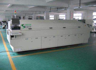

Reflow oven (provides four zones with different temperatures)
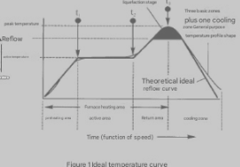
Reflow temperature curve
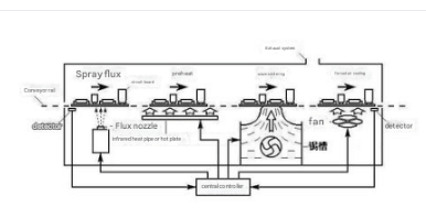
Wave soldering machine
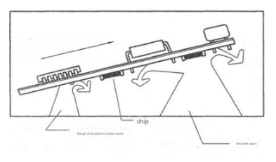
Wave soldering machine welding diagram

  • Knowing the difference between the two types of welding, you should consider which process your board will go through in the future when laying out the PCB.

If there are only SMD components, then use reflow soldering, and it is best that all components are on the same side, so that one reflow soldering can be done. If there are both SMD and plug-in components, and the pad density is not high, then use wave soldering.

Take the general home appliance PCBA as an example, it is usually a single-sided board.

In the past, it was all direct-inserted components, and then wave soldered. Now it is more common to have SMD components on the bottom and plug-in components on the front, and then wave soldered. This can reduce the area of ​​the entire PCB, and can reduce the cost of BOM (SMD resistors of the same specification are cheaper than plug-in resistors), and usually improve performance

. So I suggest that you use SMD components as much as possible. If there is no plug-in, use reflow soldering and put the components on the same side as much as possible. Otherwise, use wave soldering, place the SMD on the bottom and the plug-in on the top.

If the PCB can be designed on one side, use one side. The price of a single-sided board is about half of that of a double-sided board.

So the PCBs in the home appliances you disassemble are basically single-sided boards with plug-ins on the front and SMDs on the back.

The above summarizes the relationship between component layout selection and PCBA welding. The following will continue to summarize related knowledge, such as plug-in selection, PCB pin length, PCBA component direction, etc.~

Contact us for PCB quote now |
Post Tags: #aluminum clad pcb#aluminum core pcb#aluminum core pcb led#aluminum pcb#assemble pcb

Post navigation

Previous Previous
Streamlining PCB SMT Assembly for High-Density Circuit Design
NextContinue
Common PCB Layout Pitfalls

Search

Search

Products

  • HDI Multilayer PCB
  • Rigid Flex PCB
  • Flex pcb
  • High Frequency PCB
  • High speed pcb
  • Heavy copper PCB
  • Metal Core PCB
  • Ceramic PCB

Address

Andwin Circuits Co.,Limited
Email: sales@andwinpcb.com
Tel: +86 755 2832 9394
Fax:+86 755 2992  6717
ADD:1-2F-1217,HouDeQun Industrial park,
NanTing RD NO.56,ShaJing,BaoAn,Shenzhen 518104,GuangDong,China

Products

  • HDI Multilayer PCB
  • Rigid Flex PCB
  • Flex pcb
  • High Frequency PCB
  • High speed pcb
  • Heavy copper PCB
  • Metal Core PCB
  • Ceramic PCB

Technology

  • Blogs
  • Via in pad
  • PCB E-test
  • PCB stack up
  • Metal core PCB panelization
  • Controlled impedance PCB

CERTIFICATION

Certification >>


Copyright© 2003 - 2026 Andwin | All Rights Reserved | Powered by Andwin

Scroll to top
  • Home
  • Products
    • HDI multilayer PCB
    • Rigid Flex PCB
    • Flex pcb
    • Special PCB
      • High Frequency PCB
        • Rogers RO4350B PCB
        • Rogers RO4003 pcb
        • Rogers RO3003 PCB
        • Rogers 5880 PCB
        • DICLAD 527 PCB
        • Taconic TLX series
        • Taconic TLX-8 RF PCB
        • Taconic TLX-9 RF PCB
      • High speed pcb
        • Megtron 6 High Speed PCB
        • TU-872 SLK Sp High Speed
      • High TG PCB
        • SHENGYI SH260 PCB
        • ISOLA 370HR PCB
        • ISOLA IS410 PCB
        • ISOLA IS420 PCB
      • Heavy copper PCB
      • Copper coin pcb
      • Copper inlay PCB
    • Metal Core PCB
      • Copper core pcb
      • Aluminum PCB
      • 2 Layers Aluminum PCB
      • Direct thermal MCPCB
      • 2 Layers Direct Thermal
    • Ceramic PCB
      • DPC ceramic PCB
      • DBC ceramic PCB
      • Thick film Ceramic PCB
      • Al2O3 Alumina PCB
      • AIN ALN ceramic PCB
      • IGBT Ceramic PCB
  • Service
    • PCB Assembly
    • Quick turn PCB assembly
    • PCBA conformal coating
  • Industry
    • Telecommunication
    • IoT and Wireless
    • Industrial Control
    • Thermal management
    • Power and Energy
    • IC test board
    • Automative
    • Medical
  • Capability
    • Rigid PCB
    • Rigid flex PCB
    • Metal core PCB
    • PCB Assembly
  • Technology
    • Blogs
    • Via in pad
    • PCB E-test
    • PCB stack up
    • MCPCB panelization
    • Controlled impedance PCB
  • About
    • About us
    • Certification
    • Factory Tour
  • Contact
Search