
Skip to content
Andwin Circuits
  • Home
  • ProductsExpand
    • HDI multilayer PCB
    • Rigid Flex PCB
    • Flex pcb
    • Special PCBExpand
      • High Frequency PCBExpand
        • Rogers RO4350B PCB
        • Rogers RO4003 pcb
        • Rogers RO3003 PCB
        • Rogers 5880 PCB
        • DICLAD 527 PCB
        • Taconic TLX series
        • Taconic TLX-8 RF PCB
        • Taconic TLX-9 RF PCB
      • High speed pcbExpand
        • Megtron 6 High Speed PCB
        • TU-872 SLK Sp High Speed
      • High TG PCBExpand
        • SHENGYI SH260 PCB
        • ISOLA 370HR PCB
        • ISOLA IS410 PCB
        • ISOLA IS420 PCB
      • Heavy copper PCB
      • Copper coin pcb
      • Copper inlay PCB
    • Metal Core PCBExpand
      • Copper core pcb
      • Aluminum PCB
      • 2 Layers Aluminum PCB
      • Direct thermal MCPCB
      • 2 Layers Direct Thermal
    • Ceramic PCBExpand
      • DPC ceramic PCB
      • DBC ceramic PCB
      • Thick film Ceramic PCB
      • Al2O3 Alumina PCB
      • AIN ALN ceramic PCB
      • IGBT Ceramic PCB
  • ServiceExpand
    • PCB Assembly
    • Quick turn PCB assembly
    • PCBA conformal coating
  • IndustryExpand
    • Telecommunication
    • IoT and Wireless
    • Industrial Control
    • Thermal management
    • Power and Energy
    • IC test board
    • Automative
    • Medical
  • CapabilityExpand
    • Rigid PCB
    • Rigid flex PCB
    • Metal core PCB
    • PCB Assembly
  • TechnologyExpand
    • Blogs
    • Via in pad
    • PCB E-test
    • PCB stack up
    • MCPCB panelization
    • Controlled impedance PCB
  • AboutExpand
    • About us
    • Certification
    • Factory Tour
  • Contact
Andwin Circuits
Home / PCB modular layout ideas

PCB modular layout ideas

ByGrace July 7, 2025July 7, 2025

Facing the increasingly integrated hardware platform and increasingly complex electronic products, PCB layout should have a modular mindset, requiring modular and structured design methods to be used in both hardware schematic design and PCB wiring. As a hardware engineer, on the premise of understanding the overall system architecture, you should first consciously integrate modular design ideas in the schematic and PCB wiring design, and plan the basic ideas for PCB layout in combination with the actual situation of the PCB, as shown in Figure 1.
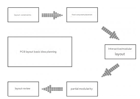
Figure 1 Basic PCB layout planning

Contact us for PCB quote now |

Placement of fixed components

The placement of fixed components is similar to the placement of fixed holes, and it also requires a precise position placement. This is mainly placed according to the design structure. The silk screen of the component and the silk screen of the structure are centered and overlapped, as shown in Figure 2. After the fixed components on the board are placed, the signal flow of the entire board can be sorted out according to the principle of flying wire proximity and signal priority.
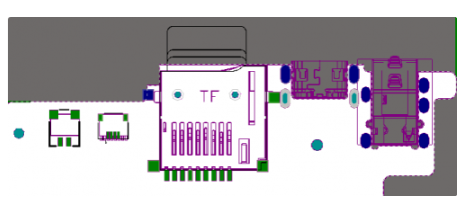
Figure 2 Placement of fixed components

Interaction settings between schematics and PCBs

In order to facilitate the search of components, it is necessary to correspond the schematics with the PCB so that the two can be mapped to each other, referred to as interaction. Interactive layout can be used to locate components relatively quickly, thereby shortening design time and improving work efficiency.

(1) In order to achieve interaction between schematics and PCB, it is necessary to execute the menu command “Tools-Cross Selection Mode” in both the schematic editing interface and the PCB design interaction interface to activate the cross selection mode, as shown in Figure 3.

(2) As shown in Figure 4, it can be seen that after selecting a component on the schematic, the corresponding component on the PCB will be selected synchronously; conversely, after selecting a component on the PCB, the corresponding component on the schematic will also be selected.
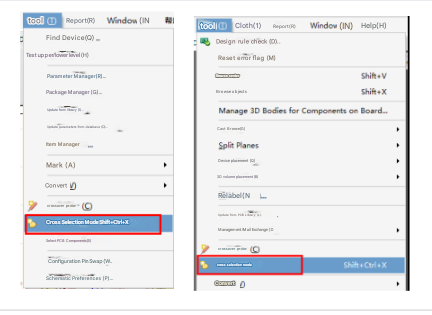
Figure 3 Activating cross selection mode
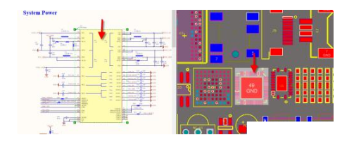
Figure 4 Selection under cross selection mode

Contact us for PCB quote now |

Modular layout

Here is a component arrangement function, that is, arranging in a rectangular area. In the early stage of layout, combined with component interaction, a bunch of messy components can be conveniently separated by module and placed in a certain area.

(1) Select all components of one module on the schematic. At this time, the components corresponding to the schematic on the PCB are selected.

(2) Execute the menu command “Tools-Device Placement-Arrange in Rectangular Area”.

(3) Select a range in a blank area on the PCB. At this time, the components of this functional module will be arranged within the selected range, as shown in Figure 5. Using this function, all functional modules on the schematic can be quickly divided into blocks.

Modular layout and interactive layout are inseparable. Using interactive layout, select all components of the module on the schematic and arrange them one by one on the PCB. Next, you can further refine the layout of ICs, resistors, and diodes. This is modular layout, and the effect diagram is shown in Figure 6.
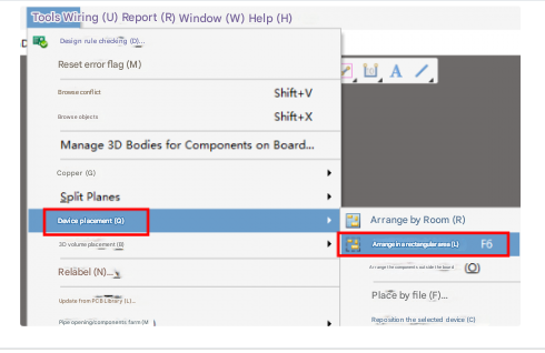
Figure 5 Arrangement in a rectangular area and arrangement of components by box selection
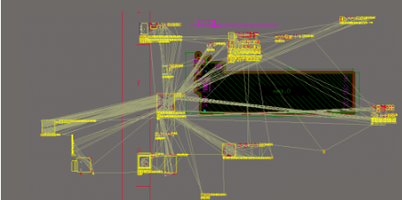
Figure 6 Modular layout effect diagram

When modular layout, you can use the “vertical split” command to split the schematic editing interface and the PCB design interaction interface, as shown in Figure 7, which makes it easier for us to view the view and quickly layout.
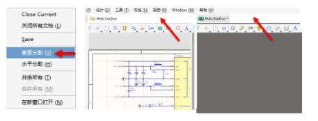
Figure 7 Split screen processing of Altium Designer

Contact us for PCB quote now |

Post Tags: #aluminum clad pcb#aluminum core pcb#aluminum pcb#assemble pcb#PCB modular layout

Post navigation

Previous Previous
Tips for Specifying PCB Hole Tolerances
NextContinue
Routing strategy in PCB Layout

Search

Search

Products

  • HDI Multilayer PCB
  • Rigid Flex PCB
  • Flex pcb
  • High Frequency PCB
  • High speed pcb
  • Heavy copper PCB
  • Metal Core PCB
  • Ceramic PCB

Address

Andwin Circuits Co.,Limited
Email: sales@andwinpcb.com
Tel: +86 755 2832 9394
Fax:+86 755 2992  6717
ADD:1-2F-1217,HouDeQun Industrial park,
NanTing RD NO.56,ShaJing,BaoAn,Shenzhen 518104,GuangDong,China

Products

  • HDI Multilayer PCB
  • Rigid Flex PCB
  • Flex pcb
  • High Frequency PCB
  • High speed pcb
  • Heavy copper PCB
  • Metal Core PCB
  • Ceramic PCB

Technology

  • Blogs
  • Via in pad
  • PCB E-test
  • PCB stack up
  • Metal core PCB panelization
  • Controlled impedance PCB

CERTIFICATION

Certification >>


Copyright© 2003 - 2026 Andwin | All Rights Reserved | Powered by Andwin

Scroll to top
  • Home
  • Products
    • HDI multilayer PCB
    • Rigid Flex PCB
    • Flex pcb
    • Special PCB
      • High Frequency PCB
        • Rogers RO4350B PCB
        • Rogers RO4003 pcb
        • Rogers RO3003 PCB
        • Rogers 5880 PCB
        • DICLAD 527 PCB
        • Taconic TLX series
        • Taconic TLX-8 RF PCB
        • Taconic TLX-9 RF PCB
      • High speed pcb
        • Megtron 6 High Speed PCB
        • TU-872 SLK Sp High Speed
      • High TG PCB
        • SHENGYI SH260 PCB
        • ISOLA 370HR PCB
        • ISOLA IS410 PCB
        • ISOLA IS420 PCB
      • Heavy copper PCB
      • Copper coin pcb
      • Copper inlay PCB
    • Metal Core PCB
      • Copper core pcb
      • Aluminum PCB
      • 2 Layers Aluminum PCB
      • Direct thermal MCPCB
      • 2 Layers Direct Thermal
    • Ceramic PCB
      • DPC ceramic PCB
      • DBC ceramic PCB
      • Thick film Ceramic PCB
      • Al2O3 Alumina PCB
      • AIN ALN ceramic PCB
      • IGBT Ceramic PCB
  • Service
    • PCB Assembly
    • Quick turn PCB assembly
    • PCBA conformal coating
  • Industry
    • Telecommunication
    • IoT and Wireless
    • Industrial Control
    • Thermal management
    • Power and Energy
    • IC test board
    • Automative
    • Medical
  • Capability
    • Rigid PCB
    • Rigid flex PCB
    • Metal core PCB
    • PCB Assembly
  • Technology
    • Blogs
    • Via in pad
    • PCB E-test
    • PCB stack up
    • MCPCB panelization
    • Controlled impedance PCB
  • About
    • About us
    • Certification
    • Factory Tour
  • Contact
Search