
PCB Solder Mask Layer Process: A Comprehensive Overview
1. Introduction
The solder mask layer is a critical component in the manufacturing of printed circuit boards (PCBs). It serves as a protective coating applied over the copper traces to prevent oxidation, avoid solder bridges during assembly, and provide electrical insulation. The solder mask also enhances the PCB’s durability and defines the areas where solder should be applied. This article explores the solder mask process, including materials, application techniques, curing methods, and quality control measures.
2. Purpose of the Solder Mask Layer
The solder mask layer fulfills several essential functions in PCB manufacturing:
- Prevents Solder Bridging: By covering non-soldering areas, the solder mask prevents unintended electrical connections caused by excess solder.
- Protects Copper Traces: It shields copper from oxidation and environmental factors such as moisture and contaminants.
- Improves Electrical Insulation: The dielectric properties of the solder mask reduce the risk of short circuits.
- Enhances Aesthetics and Readability: The solder mask provides a colored background (typically green, but also available in red, blue, black, etc.), improving component and trace visibility.
- Resists Mechanical and Chemical Damage: It protects the PCB from scratches and chemical exposure during assembly and operation.
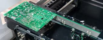
3. Solder Mask Materials
Several types of solder mask materials are used in PCB fabrication, each with distinct properties:
3.1 Liquid Photoimageable Solder Mask (LPSM)
- Applied as a liquid and then exposed to UV light through a photomask.
- Offers high precision and is suitable for fine-pitch components.
- Common types include epoxy-based and acrylic-based formulations.
3.2 Dry Film Solder Mask (DFSM)
- Comes in a solid film format and is laminated onto the PCB.
- Provides uniform thickness and is ideal for high-volume production.
- Less common than LPSM due to limitations in fine-line resolution.
3.3 Inkjet Solder Mask
- A newer technology where the solder mask is printed directly onto the PCB.
- Allows for rapid prototyping and customization.
- Still evolving in terms of material durability and resolution.
3.4 Thermal Cure and UV Cure Solder Masks
- Thermal Cure: Requires high-temperature baking to harden.
- UV Cure: Hardens under ultraviolet light, enabling faster processing.
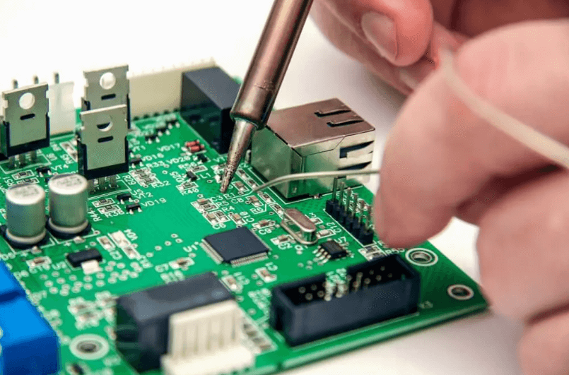
4. Solder Mask Application Process
The solder mask application involves several key steps:
4.1 Surface Preparation
Before applying the solder mask, the PCB surface must be cleaned to remove contaminants, oxidation, and residues from previous processes. Common cleaning methods include:
- Chemical Cleaning: Using alkaline or acidic solutions.
- Mechanical Scrubbing: Abrasive brushes remove surface impurities.
- Microetching: A light etch ensures optimal adhesion.
4.2 Solder Mask Coating
Depending on the material, different coating methods are used:
- Curtain Coating: A uniform layer of liquid solder mask is applied.
- Spray Coating: Used for irregular PCB shapes or selective masking.
- Screen Printing: Traditional method for low-resolution PCBs.
- Lamination (for Dry Film): The film is pressed onto the PCB under heat and pressure.
4.3 Pre-Drying (Tack Drying)
The coated PCB is partially dried to remove solvents and achieve a semi-cured state before exposure. This step prevents smearing during handling.
4.4 Exposure to UV Light
A photomask (film with the solder mask pattern) is placed over the PCB, and UV light is applied. The exposed areas polymerize and harden, while unexposed areas remain soluble.
4.5 Development
The unexposed solder mask is washed away using a developer solution (typically sodium carbonate or potassium carbonate), leaving only the cured mask on the desired areas.
4.6 Final Curing
The PCB undergoes a final cure (thermal or UV) to fully harden the solder mask, ensuring chemical and mechanical resistance.
4.7 Inspection and Quality Control
After curing, the PCB is inspected for defects such as:
- Misalignment: Incorrect solder mask registration over pads.
- Voids or Pinholes: Uncovered copper areas.
- Thickness Variations: Inconsistent coating leading to weak protection.
- Contamination: Foreign particles embedded in the mask.
Automated Optical Inspection (AOI) and manual checks ensure compliance with industry standards (IPC-SM-840).

5. Challenges in Solder Mask Application
Despite advancements, several challenges persist in solder mask processing:
5.1 Fine-Pitch Component Compatibility
As PCBs become denser with smaller components (e.g., BGA, QFN), achieving precise solder mask alignment is critical. Misalignment can lead to solder defects or poor electrical performance.
5.2 Adhesion Issues
Poor surface preparation or contamination can cause the solder mask to peel or delaminate, reducing PCB reliability.
5.3 Thermal and Mechanical Stress
The solder mask must withstand reflow soldering temperatures (up to 260°C) and mechanical stresses during assembly without cracking.
5.4 Environmental Regulations
Traditional solder masks contain solvents and chemicals that may be restricted under RoHS and REACH regulations. Manufacturers are shifting toward halogen-free and low-VOC formulations.
6. Advances in Solder Mask Technology
Recent innovations aim to improve solder mask performance:
6.1 High-Tg (Glass Transition Temperature) Solder Masks
These materials remain stable at higher temperatures, making them suitable for lead-free soldering and high-power applications.
6.2 Flexible Solder Masks for Flex PCBs
New formulations allow solder masks to bend without cracking, essential for flexible and rigid-flex PCBs.
6.3 Laser-Direct Imaging (LDI) for Solder Mask Patterning
LDI eliminates the need for photomasks by using lasers to directly expose the solder mask, improving precision and reducing waste.
6.4 Nano-Coated Solder Masks
Nanotechnology enhances solder mask properties, such as improved scratch resistance and better thermal dissipation.
7. Conclusion
The solder mask layer is a vital element in PCB manufacturing, ensuring reliability, performance, and longevity. Advances in materials and application techniques continue to address the challenges posed by miniaturization and environmental regulations. As PCB technology evolves, solder mask processes will play an increasingly critical role in enabling next-generation electronics.
By understanding the solder mask process—from material selection to quality control—manufacturers can produce high-quality PCBs that meet the demands of modern electronic devices. Future developments in eco-friendly formulations and high-resolution application methods will further enhance the capabilities of solder mask technology.