
PCB Solder Paste Stencil Design: Aperture Rules for Fine Pitch Components
When designing stencils for fine-pitch SMT assembly, getting the aperture dimensions wrong can cascade into bridging defects, insufficient paste volume, or tombstoning. After years of working with 0.4mm pitch BGAs and 0201 passives, I’ve learned that the area ratio calculation matters more than most engineers realize—and the IPC-7525C guidelines are just the starting point.
Understanding Area Ratio: The Critical Design Metric
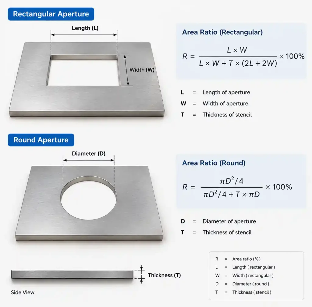
Area ratio determines whether solder paste releases cleanly from your stencil. The formula is straightforward, but its implications run deep.
For rectangular apertures:
AR = (L × W) / [2 × (L + W) × T]
For round apertures:
AR = D / (4 × T)
Where L = length, W = width, D = diameter, and T = stencil thickness.
IPC-7525C recommends a minimum area ratio of 0.66. In practice, I’ve seen successful assemblies down to 0.40 for ultra-fine pitch work—but only with laser-cut stencils, properly degassed paste, and tight process control. Going below 0.50 requires validation, not assumptions.
Stencil Thickness Selection by Component Pitch
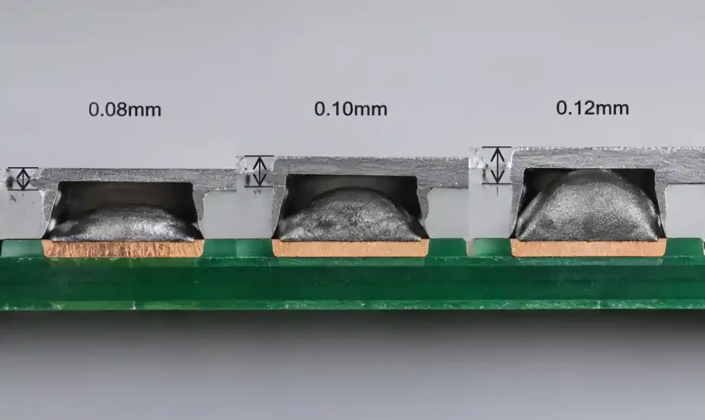
Thickness isn’t arbitrary. It directly affects paste volume and release characteristics.
| Component Pitch | Recommended Thickness | Area Ratio Target | Typical Applications |
|---|---|---|---|
| >0.5mm (Standard) | 0.12-0.15mm (5-6 mil) | ≥0.66 | Standard SMT, 0402 and larger |
| 0.4-0.5mm (Fine) | 0.10-0.12mm (4-5 mil) | 0.50-0.66 | 0.5mm BGAs, 0201 passives |
| <0.4mm (Ultra-fine) | 0.08-0.10mm (3-4 mil) | 0.40-0.50 | 0.35mm CSPs, 01005 components |
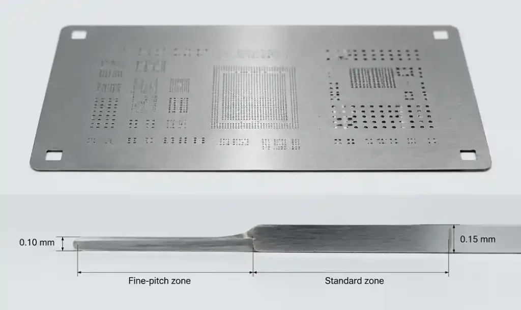
| Mixed density | Step-down design | Component-specific | QFNs with dense I/O + standard parts |
For boards mixing 0.5mm pitch QFNs with standard 0805 passives, step-down stencils solve the paste volume mismatch. Andwin Circuits fabricates step-down stencils with electropolished transitions to prevent paste wicking between thickness zones.
Aperture Design Rules for Specific Components
BGA and CSP Packages
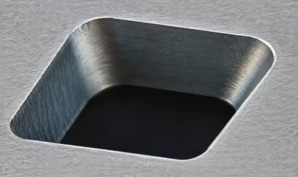
For BGAs at 0.5mm pitch and above, start with apertures at 90-95% of pad diameter. As pitch tightens to 0.4mm, reduce to 85-90% to prevent bridging. Below 0.4mm, aperture shape matters: round apertures work for 0.5mm+, but square apertures with rounded corners (0.05mm radius) improve paste release for 0.3-0.4mm pitch.
Don’t rely on aperture reduction alone. At 0.35mm pitch, even with 80% reduction and 0.10mm thickness, you’re at the edge of manufacturability. Consider NSMD pad design and verify your assembly capabilities can handle the tolerance stack.
QFN Thermal Pads
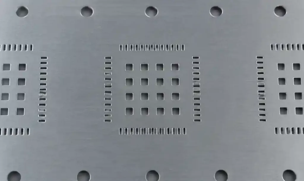
QFN thermal pads need窗口化 (windowing)—not a solid aperture. For a 5×5mm thermal pad, I use a 4×4 array of 0.8mm apertures with 0.5mm spacing. This achieves 50-60% paste coverage, prevents voiding, and avoids package flotation during reflow.
The paste volume under the thermal pad should match the perimeter lead volume. Too much paste lifts the package; too little creates thermal voids. Match your stencil thickness to the lead pitch, then window the thermal aperture accordingly.
Aperture-to-Pad Ratio Guidelines
Aperture reduction isn’t universal. Apply it where needed, not everywhere.
| Component Type | Pad Size | Aperture Reduction | Rationale |
|---|---|---|---|
| 0402 and larger passives | ≥0.5mm | 0-5% (1:1 typical) | Adequate paste volume, low bridge risk |
| 0201 passives | 0.3×0.6mm | 5-10% | Prevent tombstoning, maintain volume |
| 0.5mm pitch BGAs | 0.25-0.3mm pads | 5-10% | Balance volume and bridging |
| 0.4mm pitch BGAs | 0.20-0.25mm pads | 10-15% | Critical bridging control |
| Fine-pitch connectors (<0.5mm) | Varies | 10-15% + thickness reduction | Geometry-dependent bridging risk |
Over-reduction creates new problems. I’ve debugged cold joints on 0402s where someone applied 15% reduction “for safety”—the paste volume dropped below the minimum wetting threshold.

Calculating and Verifying Area Ratio
Walk through a real example: 0.4mm pitch BGA with 0.23mm pads, 10% aperture reduction, 0.10mm stencil thickness.
Aperture dimensions: 0.23mm × 0.9 = 0.207mm diameter
AR = D / (4 × T) = 0.207 / (4 × 0.10) = 0.207 / 0.40 = 0.518
This sits in the acceptable range for fine pitch (0.50-0.66), though it’s at the low end. In production, I’d prototype this first or consider 0.12mm thickness to push AR to 0.43—still workable with laser-cut stencils and Type 4 paste.
For rectangular pads (common on QFNs and connectors):
0.25mm × 0.80mm aperture, 0.10mm thickness
AR = (0.25 × 0.80) / [2 × (0.25 + 0.80) × 0.10] = 0.20 / 0.21 = 0.95
Excellent release characteristics. No adjustments needed.
Material and Manufacturing Considerations
Stencil material affects paste release. Laser-cut stainless steel is standard, but electropolishing the aperture walls reduces friction and improves release—critical below 0.5mm pitch. Nano-coatings further reduce surface energy, but validate compatibility with your paste chemistry.
Solder paste type must match your design. Type 4 or Type 5 paste (25-38μm or 15-25μm powder) is non-negotiable for fine pitch. Type 3 paste (25-45μm) bridges at 0.5mm pitch and below. Andwin Circuits validates stencil designs against customer-specified paste types before fabrication.
Aperture taper from laser cutting should be 92-95° (slightly trapezoidal, wider on print side). Perfectly vertical walls (90°) can trap paste; excessive taper (>95°) reduces effective thickness. Request aperture profile inspection for critical fine-pitch designs.
Common Design Mistakes and How to Avoid Them
Mistake 1: Using the same thickness for all components
Mixed-density boards need step-down stencils. Don’t compromise 0402 passive paste volume to accommodate a 0.4mm BGA—use localized thickness reduction.
Mistake 2: Ignoring paste type in area ratio calculations
Type 4 paste releases better than Type 3 at the same area ratio. A 0.55 AR with Type 4 paste outperforms 0.65 AR with Type 3 paste at fine pitch.
Mistake 3: Applying pad reduction to all components
Start with 1:1 apertures for standard components (≥0.5mm pitch, ≥0.5mm pads). Apply reduction only where bridging risk exists—BGAs, fine-pitch connectors, closely-spaced leads.
Mistake 4: Forgetting to validate calculated values
Area ratio above 0.66 doesn’t guarantee success if your aperture dimensions create paste slump or if your reflow profile is wrong. Prototype critical designs with SPI (solder paste inspection) verification.
Advanced Techniques for Ultra-Fine Pitch
When component pitch drops to 0.3mm, standard approaches fail. Here’s what works:
Hybrid stencil designs: Combine electroformed nickel (ultra-smooth walls) in fine-pitch zones with laser-cut stainless steel for standard areas. Electroformed stencils are expensive but justify the cost for 0.3mm pitch and below.
Dynamic stencil printing: Some paste dispensing systems use programmable squeegee pressure and print speed per board zone. For ultra-fine pitch, slower print speed (20-30mm/s vs. 50-80mm/s standard) improves fill without increasing thickness.
ENIG pad finish validation: Area ratio calculations assume ideal pad wetting. ENIG surface contamination or black pad defects kill fine-pitch yield. Specify controlled impedance PCB processes with validated pad finishes.
FAQs
What’s the minimum area ratio for reliable paste release?
IPC-7525C specifies 0.66, but modern Type 4/5 pastes and laser-cut stencils achieve reliable release down to 0.50 for fine pitch, and 0.40 for ultra-fine pitch under controlled conditions. Below 0.50 requires process validation with your specific paste and equipment.
Should I use round or square apertures for fine-pitch BGAs?
Round apertures work well for 0.5mm pitch and above. For 0.4mm pitch and below, square apertures with 0.05mm corner radius provide better paste volume consistency and reduced bridging risk compared to pure round apertures at equivalent area ratios.
How do I handle mixed-component densities on one board?
Step-down stencils with localized thickness reductions solve this. Place fine-pitch components in a 0.10mm zone and standard components in a 0.12-0.15mm zone. The transition should be electropolished to prevent paste wicking between zones.
Can I use the same stencil thickness for 0201 passives and 0.5mm BGAs?
Yes, but verify area ratios for both. At 0.12mm thickness, 0201 passives (0.30×0.60mm pads) achieve AR ≈ 0.63 with 1:1 apertures, and 0.5mm BGAs with 0.27mm pads achieve AR ≈ 0.56 with 10% reduction. Both are acceptable. If either falls below 0.50, adjust thickness or aperture sizing.
What paste type should I specify for 0.4mm pitch components?
Type 4 (25-38μm powder) minimum. Type 5 (15-25μm) improves fine-pitch performance but requires tighter humidity control and shorter stencil life. Avoid Type 3 paste (25-45μm) for anything below 0.5mm pitch—the powder size causes bridging.
How much aperture reduction should I apply to QFN leads?
For QFN perimeter leads at 0.5mm pitch, start with 10% reduction (0.90× pad size). At 0.4mm pitch, use 10-15% reduction. For the thermal pad, don’t reduce—use windowing (multiple smaller apertures) to achieve 50-60% paste coverage instead.
Conclusion
Fine-pitch stencil design is deterministic, not guesswork. Area ratio, aperture dimensions, and thickness must be calculated together—not independently. IPC-7525C provides the framework, but real-world success requires matching stencil parameters to your specific paste type, PCB finish, and assembly process capabilities.
For components at 0.4mm pitch and below, validate designs with prototype builds before committing to production. Small dimensional errors at fine pitch amplify into yield problems. Work with your PCB manufacturer and assembly partner early to review stencil designs against their process capabilities—especially for step-down stencils and ultra-fine pitch applications.
The difference between a 0.50 and 0.55 area ratio may seem trivial, but at 0.35mm pitch with hundreds of solder joints, it’s the difference between 98% and 85% yield.