Skip to content
Andwin Circuits
  • Home
  • ProductsExpand
    • HDI multilayer PCB
    • Rigid Flex PCB
    • Flex pcb
    • Special PCBExpand
      • High Frequency PCBExpand
        • Rogers RO4350B PCB
        • Rogers RO4003 pcb
        • Rogers RO3003 PCB
        • Rogers 5880 PCB
        • DICLAD 527 PCB
        • Taconic TLX series
        • Taconic TLX-8 RF PCB
        • Taconic TLX-9 RF PCB
      • High speed pcbExpand
        • Megtron 6 High Speed PCB
        • TU-872 SLK Sp High Speed
      • High TG PCBExpand
        • SHENGYI SH260 PCB
        • ISOLA 370HR PCB
        • ISOLA IS410 PCB
        • ISOLA IS420 PCB
      • Heavy copper PCB
      • Copper coin pcb
      • Copper inlay PCB
    • Metal Core PCBExpand
      • Copper core pcb
      • Aluminum PCB
      • 2 Layers Aluminum PCB
      • Direct thermal MCPCB
      • 2 Layers Direct Thermal
    • Ceramic PCBExpand
      • DPC ceramic PCB
      • DBC ceramic PCB
      • Thick film Ceramic PCB
      • Al2O3 Alumina PCB
      • AIN ALN ceramic PCB
      • IGBT Ceramic PCB
  • ServiceExpand
    • PCB Assembly
    • Quick turn PCB assembly
    • PCBA conformal coating
  • IndustryExpand
    • Telecommunication
    • IoT and Wireless
    • Industrial Control
    • Thermal management
    • Power and Energy
    • IC test board
    • Automative
    • Medical
  • CapabilityExpand
    • Rigid PCB
    • Rigid flex PCB
    • Metal core PCB
    • PCB Assembly
  • TechnologyExpand
    • Blogs
    • Via in pad
    • PCB E-test
    • PCB stack up
    • MCPCB panelization
    • Controlled impedance PCB
  • AboutExpand
    • About us
    • Certification
    • Factory Tour
  • Contact
Andwin Circuits
Home / PCB Testability Design Key Points Introduction

PCB Testability Design Key Points Introduction

ByGrace June 24, 2025June 24, 2025

1. Introduction

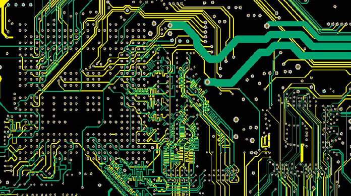
Printed Circuit Board (PCB) testability is a critical aspect of modern electronics design, ensuring that a board can be efficiently tested for defects during manufacturing and throughout its lifecycle. Effective testability design reduces production costs, improves yield, and enhances reliability. This article explores key PCB testability design considerations, including Design for Test (DFT) strategies, test point placement, boundary scan, and automated test equipment (ATE) compatibility.

2. Importance of PCB Testability

A well-designed PCB must be testable to:

  • Detect manufacturing defects (shorts, opens, missing components).
  • Verify functionality (signal integrity, power delivery).
  • Reduce debugging time during prototyping and production.
  • Lower costs by minimizing rework and scrap.

Without proper testability, defects may go undetected, leading to field failures and increased warranty costs.

Contact us for PCB quote now |

3. Key PCB Testability Design Points

3.1 Design for Test (DFT) Principles

DFT involves designing PCBs to facilitate testing. Key principles include:

  • Accessibility: Test points should be easily reachable by probes.
  • Visibility: Critical signals should be observable.
  • Controllability: Test signals should be injectable for validation.

3.2 Test Point Placement

  • Spacing: Test points should be spaced adequately (typically ≥ 0.1 inches apart) for probe access.
  • Location: Place test points near components under test (e.g., ICs, connectors).
  • Avoid Obstructions: Keep test points away from tall components that may block probes.

3.3 Boundary Scan (JTAG/IEEE 1149.1)

  • Purpose: Enables testing of interconnects and IC functionality without physical probes.
  • Implementation:
  • Include JTAG-compliant components (e.g., microcontrollers, FPGAs).
  • Ensure proper TAP (Test Access Port) connections (TDI, TDO, TCK, TMS).
  • Benefits: Reduces dependency on physical test points for complex boards.

3.4 In-Circuit Test (ICT) Compatibility

  • Test Pads: Provide dedicated test pads for ICT bed-of-nails fixtures.
  • Avoid Solder Mask Over Test Points: Ensure test points are exposed for probe contact.
  • Power & Ground Access: Include test points for power rails to detect shorts.

3.5 Flying Probe Test Considerations

  • No Fixture Needed: Suitable for low-volume production.
  • Test Point Size: ≥ 20 mil diameter for reliable contact.
  • Avoid High-Density Clustering: Prevents probe collision risks.

3.6 Functional Test (FCT) Support

  • Test Connectors: Include headers for functional test interfaces.
  • Firmware Hooks: Design firmware to support test mode commands.
  • Signal Probing Points: Provide access to high-speed signals (e.g., USB, PCIe) for validation.

3.7 Built-In Self-Test (BIST) Features

  • Memory BIST: For RAM/Flash testing.
  • Logic BIST: For FPGA/ASIC self-validation.
  • Analog BIST: For ADC/DAC and power supply monitoring.

3.8 Power Distribution Testability

  • Test Points for All Rails: Ensure access to 3.3V, 5V, 12V, etc.
  • Current Measurement Points: Include shunt resistors or test pads for current sensing.

3.9 Signal Integrity & Testability

  • Impedance Control: Ensure controlled impedance for high-speed signals.
  • Test Points for Critical Signals: Provide access to clocks, data lines, and control signals.

3.10 Design Documentation for Testability

  • Test Strategy Document: Outline test coverage requirements.
  • Schematic Annotations: Mark test points and critical nets.
  • Gerber Layer for Test Points: Helps test engineers locate probe points.
Contact us for PCB quote now |

4. Common PCB Testability Mistakes to Avoid

  • Insufficient Test Points: Leads to low fault coverage.
  • Poor Probe Accessibility: Test points blocked by components.
  • Ignoring JTAG/Boundary Scan: Misses opportunities for digital interconnect testing.
  • Overlooking Power Network Testability: Undetected power shorts increase failure rates.

5. Conclusion

PCB testability design is essential for manufacturing efficiency, reliability, and cost reduction. By incorporating DFT principles, optimizing test point placement, leveraging boundary scan, and ensuring compatibility with ICT and flying probe testing, designers can significantly improve test coverage and defect detection. A well-documented test strategy further enhances the testing process, ensuring high-quality PCB production.

By following these guidelines, engineers can design PCBs that are not only functional but also easy to validate and troubleshoot, leading to faster time-to-market and higher product reliability.

Contact us for PCB quote now |

Post Tags: #aluminum clad pcb#aluminum core pcb#aluminum pcb#assemble pcb#PCB Testability

Post navigation

Previous Previous
How to Thicken Power Traces in PCB Design: A Comprehensive Guide
NextContinue
Understanding Reverse Positioning in the PCB Clone Market

Search

Search

Products

  • HDI Multilayer PCB
  • Rigid Flex PCB
  • Flex pcb
  • High Frequency PCB
  • High speed pcb
  • Heavy copper PCB
  • Metal Core PCB
  • Ceramic PCB

Address

Andwin Circuits Co.,Limited
Email: sales@andwinpcb.com
Tel: +86 755 2832 9394
Fax:+86 755 2992  6717
ADD:1-2F-1217,HouDeQun Industrial park,
NanTing RD NO.56,ShaJing,BaoAn,Shenzhen 518104,GuangDong,China

Products

  • HDI Multilayer PCB
  • Rigid Flex PCB
  • Flex pcb
  • High Frequency PCB
  • High speed pcb
  • Heavy copper PCB
  • Metal Core PCB
  • Ceramic PCB

Technology

  • Blogs
  • Via in pad
  • PCB E-test
  • PCB stack up
  • Metal core PCB panelization
  • Controlled impedance PCB

CERTIFICATION

Certification >>


Copyright© 2003 - 2026 Andwin | All Rights Reserved | Powered by Andwin

Scroll to top
  • Home
  • Products
    • HDI multilayer PCB
    • Rigid Flex PCB
    • Flex pcb
    • Special PCB
      • High Frequency PCB
        • Rogers RO4350B PCB
        • Rogers RO4003 pcb
        • Rogers RO3003 PCB
        • Rogers 5880 PCB
        • DICLAD 527 PCB
        • Taconic TLX series
        • Taconic TLX-8 RF PCB
        • Taconic TLX-9 RF PCB
      • High speed pcb
        • Megtron 6 High Speed PCB
        • TU-872 SLK Sp High Speed
      • High TG PCB
        • SHENGYI SH260 PCB
        • ISOLA 370HR PCB
        • ISOLA IS410 PCB
        • ISOLA IS420 PCB
      • Heavy copper PCB
      • Copper coin pcb
      • Copper inlay PCB
    • Metal Core PCB
      • Copper core pcb
      • Aluminum PCB
      • 2 Layers Aluminum PCB
      • Direct thermal MCPCB
      • 2 Layers Direct Thermal
    • Ceramic PCB
      • DPC ceramic PCB
      • DBC ceramic PCB
      • Thick film Ceramic PCB
      • Al2O3 Alumina PCB
      • AIN ALN ceramic PCB
      • IGBT Ceramic PCB
  • Service
    • PCB Assembly
    • Quick turn PCB assembly
    • PCBA conformal coating
  • Industry
    • Telecommunication
    • IoT and Wireless
    • Industrial Control
    • Thermal management
    • Power and Energy
    • IC test board
    • Automative
    • Medical
  • Capability
    • Rigid PCB
    • Rigid flex PCB
    • Metal core PCB
    • PCB Assembly
  • Technology
    • Blogs
    • Via in pad
    • PCB E-test
    • PCB stack up
    • MCPCB panelization
    • Controlled impedance PCB
  • About
    • About us
    • Certification
    • Factory Tour
  • Contact
Search