Understanding Reverse Positioning in the PCB Clone Market
Introduction
The printed circuit board (PCB) industry is a critical component of modern electronics, serving as the backbone for devices ranging from consumer electronics to industrial machinery. Within this industry, PCB cloning—also known as PCB reverse engineering or PCB copy—has emerged as a controversial yet significant segment. Reverse positioning in the PCB clone market refers to the strategic approach of analyzing and replicating existing PCB designs rather than innovating from scratch. This practice is often employed for competitive benchmarking, legacy system maintenance, or cost reduction.
This article explores the concept of reverse positioning in the PCB clone market, examining its ethical, legal, and technical dimensions. We will discuss why companies engage in PCB cloning, the methodologies used, the challenges involved, and the future outlook of this market.
The Concept of Reverse Positioning in PCB Cloning
Reverse positioning in PCB cloning involves studying an existing PCB design to recreate or improve upon it without direct access to the original design files. Unlike traditional PCB design, which follows a forward engineering process (from schematic to layout to production), reverse engineering starts with the physical PCB and works backward to extract its design parameters.
Key Motivations for PCB Cloning
- Legacy System Maintenance
- Many industries rely on outdated electronics where original design files are lost or manufacturers no longer exist. PCB cloning allows companies to reproduce obsolete boards to extend the lifespan of critical equipment.
- Competitive Benchmarking
- Companies may analyze competitors’ PCBs to understand design choices, component selection, and manufacturing techniques, helping them improve their own products.
- Cost Reduction
- Instead of investing in expensive R&D, some firms clone proven designs to reduce development time and costs.
- Intellectual Property (IP) Verification
- In some cases, companies use reverse engineering to verify whether a competitor’s product infringes on their patents.
Methodologies of PCB Reverse Engineering
The PCB cloning process involves several technical steps:
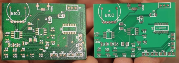
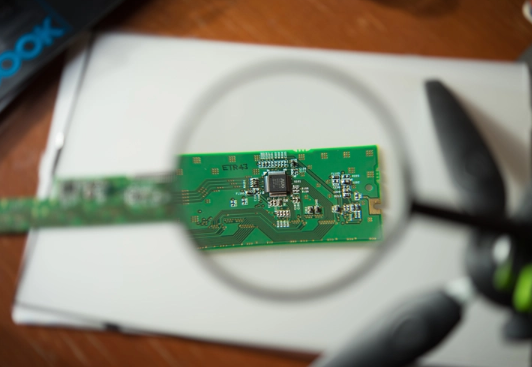
1. Physical PCB Analysis
- The first step is to obtain a sample of the target PCB. High-resolution imaging, X-ray scanning, and microscopy may be used to examine layer stacking and trace routing.
2. Schematic Reconstruction
- Using specialized software, engineers extract netlists and component connections to reconstruct the circuit schematic.
3. Component Identification
- Identifying components (ICs, resistors, capacitors) is crucial. Decapping (removing IC packaging to examine silicon dies) may be necessary for proprietary chips.
4. PCB Layout Recreation
- Once the schematic is understood, engineers recreate the PCB layout using EDA (Electronic Design Automation) tools like Altium Designer or KiCad.
5. Prototyping and Testing
- The cloned design is fabricated and tested to ensure functionality matches the original.
Legal and Ethical Considerations
PCB cloning operates in a legal gray area, depending on jurisdiction and intent:
- Patent and Copyright Issues
- Copying a PCB design may infringe on intellectual property rights if the original is patented. However, some jurisdictions allow reverse engineering for interoperability or research purposes (e.g., under fair use in the U.S.).
- Ethical Dilemmas
- While cloning for repair or compatibility is often seen as acceptable, using reverse engineering to steal trade secrets is unethical and potentially illegal.
- Regulatory Compliance
- Industries like defense and aerospace have strict regulations against unauthorized PCB duplication due to security concerns.
Challenges in PCB Reverse Engineering
- Complex Multi-Layer Boards
- Modern PCBs with high-density interconnects (HDI) and blind/buried vias are difficult to reverse engineer without advanced equipment.
- Encrypted or Obfuscated Designs
- Some manufacturers use security measures like tamper-resistant coatings or encrypted firmware to deter cloning.
- Component Obsolescence
- Even if a PCB is cloned, sourcing obsolete components can be a challenge.
- Legal Risks
- Companies engaging in cloning must navigate IP laws carefully to avoid litigation.
The Future of PCB Reverse Engineering
As technology evolves, so do the tools and techniques for PCB cloning:
- AI-Assisted Reverse Engineering
- Machine learning can automate trace recognition and component matching, speeding up the process.
- 3D X-Ray Tomography
- Advanced imaging allows non-destructive analysis of multi-layer PCBs.
- Blockchain for IP Protection
- Some companies are exploring blockchain to timestamp and verify PCB designs, making unauthorized cloning harder.
Conclusion
Reverse positioning in the PCB clone market is a double-edged sword—it enables innovation and legacy support but also raises ethical and legal concerns. While the practice is unlikely to disappear, its future will depend on advancements in anti-cloning technologies, evolving IP laws, and industry self-regulation. Companies must weigh the benefits of reverse engineering against potential risks, ensuring compliance while leveraging cloning for legitimate purposes.
As the electronics industry continues to grow, the debate over PCB cloning will persist, balancing between competition, innovation, and intellectual property protection.