
PCB Ultrasonic Cleaner: Revolutionizing Cleaning in Electronics Manufacturing
Introduction
In the realm of electronics manufacturing, the production of Printed Circuit Boards (PCBs) is a critical process that demands precision, cleanliness, and efficiency. PCBs are the backbone of virtually all electronic devices, from smartphones and computers to medical equipment and automotive systems. As the complexity and miniaturization of electronic components continue to advance, the need for effective cleaning solutions has become more pronounced. One such solution that has gained significant traction in recent years is the PCB ultrasonic cleaner. This article delves into the intricacies of PCB ultrasonic cleaners, exploring their working principles, benefits, applications, and future prospects.
Understanding PCBs and the Need for Cleaning
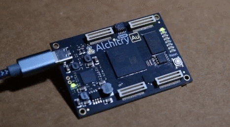
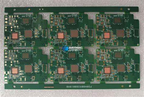
Before delving into the specifics of ultrasonic cleaning, it is essential to understand the nature of PCBs and why cleaning is crucial in their manufacturing process. PCBs are composed of a non-conductive substrate, typically made of fiberglass or composite epoxy, with conductive pathways etched or printed onto the surface. These pathways, known as traces, connect various electronic components such as resistors, capacitors, and integrated circuits (ICs) to form a functional electronic circuit.
During the manufacturing process, PCBs are subjected to various stages, including etching, soldering, and assembly. Each of these stages can introduce contaminants such as flux residues, solder paste, dust, and oils. If left uncleaned, these contaminants can lead to several issues, including:
- Electrical Shorts: Contaminants can create unintended conductive paths, leading to short circuits and potential device failure.
- Corrosion: Residual flux and other chemicals can corrode metal components, compromising the integrity and longevity of the PCB.
- Poor Adhesion: Contaminants can interfere with the adhesion of conformal coatings, which are applied to protect the PCB from environmental factors such as moisture and dust.
- Aesthetic Issues: Visible contaminants can detract from the overall appearance of the PCB, which may be a concern for consumer electronics.
Given these potential issues, effective cleaning of PCBs is paramount to ensure their reliability, performance, and longevity.
The Emergence of Ultrasonic Cleaning
Traditional cleaning methods for PCBs, such as manual brushing, solvent washing, and spray cleaning, have been widely used for decades. However, these methods have limitations, particularly when it comes to cleaning complex and densely populated PCBs with fine-pitch components. Manual cleaning is labor-intensive and prone to human error, while solvent washing and spray cleaning may not effectively remove contaminants from hard-to-reach areas.
Ultrasonic cleaning has emerged as a superior alternative, offering a more efficient and thorough cleaning solution. This technology utilizes high-frequency sound waves to generate microscopic bubbles in a cleaning solution, a phenomenon known as cavitation. These bubbles implode upon contact with the PCB surface, creating intense localized pressure and turbulence that dislodges contaminants from even the most intricate geometries.
How PCB Ultrasonic Cleaners Work
PCB ultrasonic cleaners consist of several key components:
- Ultrasonic Transducer: The transducer is the heart of the ultrasonic cleaner, converting electrical energy into high-frequency sound waves. These sound waves are typically in the range of 20 kHz to 80 kHz, with higher frequencies being more suitable for delicate components.
- Cleaning Tank: The cleaning tank holds the cleaning solution and the PCBs to be cleaned. It is designed to withstand the corrosive effects of the cleaning agents and the mechanical action of cavitation.
- Cleaning Solution: The choice of cleaning solution depends on the type of contaminants and the materials of the PCB. Common cleaning agents include deionized water, isopropyl alcohol, and specialized flux removers.
- Heating Element: Some ultrasonic cleaners are equipped with heating elements to warm the cleaning solution, enhancing its effectiveness by increasing the solubility of contaminants.
- Control Panel: The control panel allows operators to adjust parameters such as cleaning time, temperature, and ultrasonic frequency.
The cleaning process typically involves the following steps:
- Preparation: The PCBs are placed in the cleaning tank, ensuring that they are fully submerged in the cleaning solution.
- Ultrasonic Cleaning: The ultrasonic transducer is activated, generating sound waves that create cavitation bubbles in the cleaning solution. These bubbles implode, dislodging contaminants from the PCB surface.
- Rinsing: After ultrasonic cleaning, the PCBs are rinsed with deionized water or another suitable rinsing agent to remove any residual cleaning solution and contaminants.
- Drying: The cleaned PCBs are dried using methods such as air drying, heated drying, or vacuum drying to prevent water spots and ensure a clean, dry surface.
Advantages of PCB Ultrasonic Cleaners
PCB ultrasonic cleaners offer several advantages over traditional cleaning methods, making them an indispensable tool in modern electronics manufacturing:
- Superior Cleaning Performance: Ultrasonic cleaning is highly effective at removing contaminants from complex and densely populated PCBs, including hard-to-reach areas such as under components and within vias.
- Consistency and Repeatability: Ultrasonic cleaners provide consistent cleaning results, reducing the variability associated with manual cleaning methods. This consistency is crucial for maintaining high-quality standards in PCB production.
- Time Efficiency: Ultrasonic cleaning is significantly faster than manual cleaning, allowing for higher throughput and reduced production times.
- Environmental Benefits: Many ultrasonic cleaners use environmentally friendly cleaning solutions, reducing the need for hazardous chemicals and minimizing the environmental impact of PCB manufacturing.
- Cost-Effectiveness: While the initial investment in an ultrasonic cleaner may be higher than traditional cleaning equipment, the long-term cost savings in labor, cleaning agents, and reduced rework make it a cost-effective solution.
- Versatility: Ultrasonic cleaners can be used for a wide range of PCB types and sizes, making them a versatile tool for electronics manufacturers.
Applications of PCB Ultrasonic Cleaners
PCB ultrasonic cleaners are used in various stages of PCB manufacturing and assembly, including:
- Post-Etching Cleaning: After the etching process, PCBs may have residual etching chemicals and debris that need to be removed to ensure proper functionality.
- Post-Soldering Cleaning: Soldering can leave behind flux residues and solder splatter, which can be effectively removed using ultrasonic cleaning.
- Pre-Coating Cleaning: Before applying conformal coatings or other protective layers, PCBs must be thoroughly cleaned to ensure proper adhesion and performance.
- Rework and Repair: Ultrasonic cleaning is also used in the rework and repair of PCBs, removing contaminants from previously assembled boards.
- Medical and Aerospace Applications: In industries where reliability is critical, such as medical devices and aerospace, ultrasonic cleaning ensures that PCBs meet stringent cleanliness standards.
Challenges and Considerations
While PCB ultrasonic cleaners offer numerous benefits, there are some challenges and considerations to keep in mind:
- Component Sensitivity: High-frequency ultrasonic cleaning can be too aggressive for certain delicate components, potentially causing damage. It is essential to select the appropriate frequency and cleaning parameters to avoid harming sensitive parts.
- Cleaning Solution Compatibility: The cleaning solution must be compatible with the materials used in the PCB and its components. Incompatible solutions can cause corrosion or other damage.
- Maintenance: Ultrasonic cleaners require regular maintenance, including cleaning the tank, replacing the cleaning solution, and inspecting the transducer, to ensure optimal performance.
- Initial Investment: The upfront cost of an ultrasonic cleaner can be significant, particularly for high-end models with advanced features. However, the long-term benefits often justify the investment.
Future Trends in PCB Ultrasonic Cleaning
As the electronics industry continues to evolve, so too will the technology and methods used for PCB cleaning. Several trends are likely to shape the future of PCB ultrasonic cleaners:
- Miniaturization and Higher Frequencies: As PCBs become more compact and components more densely packed, ultrasonic cleaners will need to operate at higher frequencies to effectively clean these intricate designs without causing damage.
- Green Cleaning Solutions: There is a growing emphasis on environmentally friendly cleaning solutions that minimize the use of hazardous chemicals and reduce the environmental impact of PCB manufacturing.
- Automation and Integration: The integration of ultrasonic cleaners into automated PCB assembly lines will become more prevalent, allowing for seamless cleaning processes that enhance efficiency and reduce human intervention.
- Advanced Monitoring and Control: Future ultrasonic cleaners may incorporate advanced sensors and control systems to monitor cleaning parameters in real-time, ensuring optimal cleaning performance and reducing the risk of damage to sensitive components.
- Customization and Flexibility: As the diversity of PCB designs and materials continues to grow, ultrasonic cleaners will need to offer greater customization and flexibility to accommodate a wide range of cleaning requirements.
Conclusion
PCB ultrasonic cleaners have revolutionized the way PCBs are cleaned in the electronics manufacturing industry. By leveraging the power of ultrasonic cavitation, these cleaners offer superior cleaning performance, consistency, and efficiency compared to traditional methods. As the demand for more complex and miniaturized electronic devices continues to rise, the importance of effective PCB cleaning cannot be overstated. With ongoing advancements in ultrasonic cleaning technology, the future holds exciting possibilities for further enhancing the cleanliness, reliability, and performance of PCBs in a wide range of applications. Whether in consumer electronics, medical devices, or aerospace systems, PCB ultrasonic cleaners will remain a critical tool in ensuring the quality and longevity of electronic products.