
POWER PCB Inner Layer Segmentation and Copper Pour Techniques
Abstract
Printed Circuit Board (PCB) design for high-power applications requires careful consideration of power distribution, thermal management, and signal integrity. One of the critical aspects of designing such PCBs is the proper segmentation of inner power planes and effective copper pour techniques. This paper discusses the methodologies for inner layer segmentation in POWER PCBs, the benefits of copper pouring, and best practices to ensure optimal performance. Key topics include power plane splitting, thermal relief, anti-copper island strategies, and design considerations for minimizing electromagnetic interference (EMI).
1. Introduction
Modern electronic systems demand efficient power delivery networks (PDNs) to support high-current applications. Multi-layer PCBs often incorporate dedicated power and ground planes to ensure stable voltage distribution and reduce noise. However, when multiple voltage levels coexist on the same layer, proper segmentation of the inner power planes becomes essential. Additionally, copper pouring—a technique where large areas of the PCB are filled with conductive material—enhances heat dissipation and reduces impedance.
This paper explores the techniques for inner layer segmentation and copper pouring in POWER PCBs, addressing design challenges and providing practical solutions.
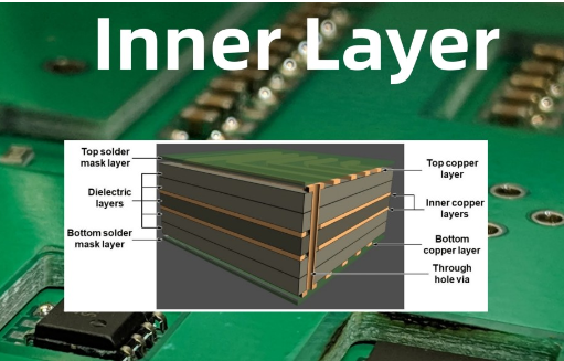
2. Inner Layer Segmentation in POWER PCBs
2.1 Purpose of Power Plane Segmentation
In complex PCBs, different components may require different supply voltages (e.g., 3.3V, 5V, 12V). Instead of dedicating separate layers for each voltage, designers often split a single plane into multiple isolated regions. Proper segmentation ensures:
- Minimized Crosstalk: Prevents noise coupling between different power domains.
- Improved Current Handling: Ensures sufficient copper area for high-current paths.
- Thermal Management: Helps distribute heat more evenly.
2.2 Techniques for Power Plane Splitting
(1) Physical Segmentation Using Keep-Out Zones
Designers define boundaries between different voltage regions using keep-out lines. These prevent accidental copper connections between adjacent power nets.
(2) Dynamic Copper Balancing
To avoid uneven current distribution, copper areas should be balanced. If one section carries higher current, its copper area should be proportionally larger.
(3) Use of Split Planes in CAD Tools
Modern PCB design software (e.g., Altium Designer, Cadence Allegro) allows dynamic power plane splitting. Designers can draw split lines to isolate different voltage regions while maintaining design rule checks (DRC).
2.3 Challenges in Inner Layer Segmentation
- Signal Integrity Issues: Improper splits can create return path discontinuities, leading to EMI.
- Manufacturing Constraints: Excessively thin copper traces between splits may lead to etching errors.
- Thermal Imbalance: Uneven copper distribution can cause localized heating.
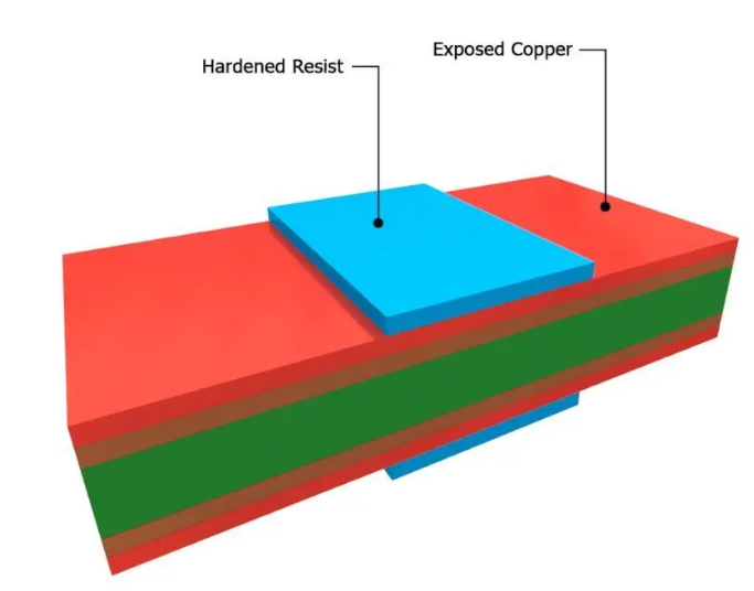
3. Copper Pour Techniques in POWER PCBs
3.1 Benefits of Copper Pour
- Enhanced Heat Dissipation: Large copper areas act as heat sinks.
- Reduced Ground Impedance: Improves signal return paths.
- EMI Shielding: Helps contain electromagnetic radiation.
3.2 Copper Pour Strategies
(1) Solid Copper Pour
A continuous copper fill provides the lowest impedance and best thermal performance. However, it may lead to warping during reflow soldering due to uneven thermal expansion.
(2) Cross-Hatched Copper Pour
A grid-like pattern reduces thermal stress but increases impedance. Useful for flexible PCBs where mechanical bending is a concern.
(3) Thermal Relief Connections
When connecting copper pours to vias or pads, thermal relief spokes prevent excessive heat transfer during soldering, improving manufacturability.
3.3 Anti-Copper Island Techniques
Unconnected copper islands can act as antennas, radiating EMI. To prevent this:
- Use “Remove Dead Copper” options in PCB design software.
- Ensure all copper regions are properly connected to a net.
4. Design Considerations for Optimal Performance
4.1 Current Carrying Capacity
Copper thickness (e.g., 1oz vs. 2oz) impacts current handling. Wider traces and larger copper areas reduce resistive losses.
4.2 Return Path Management
High-speed signals require uninterrupted return paths. Avoid splitting ground planes beneath critical signal traces.
4.3 Thermal Analysis
Simulation tools (e.g., Ansys Icepak) help predict hot spots and optimize copper pour distribution.
5. Case Study: Multi-Rail Power PCB Design
A 4-layer PCB with 3.3V, 5V, and 12V power rails was designed using Altium Designer. Key steps included:
- Power Plane Segmentation: Split the inner layer into three isolated regions.
- Copper Pour Application: Solid copper pour for ground planes, cross-hatched for power planes.
- Thermal Relief Implementation: Added spoke connections for all through-hole components.
Results showed a 20% reduction in thermal resistance and 15% lower EMI emissions compared to a non-optimized design.
6. Conclusion
Effective inner layer segmentation and copper pouring are crucial for high-performance POWER PCBs. By following best practices in plane splitting, thermal management, and EMI reduction, designers can achieve robust and reliable power distribution networks. Future advancements in CAD tools and simulation software will further enhance these techniques, enabling even more efficient PCB designs.