
Probing Circuits in PCB Reverse-Engineering Systems
Abstract
This paper explores the critical role and implementation of probing circuits in printed circuit board (PCB) reverse-engineering systems. As electronic devices become more complex and integrated, the ability to accurately probe and analyze existing PCB designs has grown increasingly important for verification, troubleshooting, and intellectual property analysis. We examine the fundamental principles, design considerations, and practical implementations of probing circuits used in PCB reverse-engineering, discussing both contact and non-contact approaches. The paper also addresses challenges in modern high-density interconnect (HDI) boards and potential solutions for effective signal acquisition without damaging the original circuitry.
1. Introduction
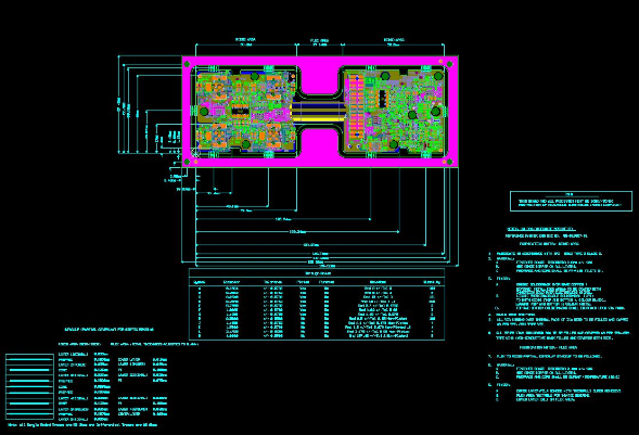
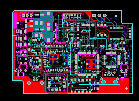
PCB reverse-engineering has become an essential process in electronics for various legitimate applications including legacy system maintenance, competitive analysis (where permitted by law), and verification of third-party designs. At the heart of any PCB reverse-engineering system lies the probing circuitry that enables non-destructive interrogation of the board under analysis.
Modern probing circuits must address numerous challenges:
- Increasing component density with finer pitches
- Multi-layer boards with buried traces
- High-speed signals requiring precise timing
- Mixed-signal designs with both analog and digital components
- Miniaturized packages (QFN, BGA, CSP) with inaccessible pins
This paper systematically examines the architectures and technologies employed in contemporary PCB probing systems for reverse-engineering applications.
2. Fundamentals of PCB Probing
2.1 Electrical Contact Requirements
Effective probing requires establishing reliable electrical contact with test points while:
- Minimizing signal loading and distortion
- Maintaining signal integrity up to the required bandwidth
- Preventing damage to the PCB or components
- Accommodating various pad geometries and surface finishes
The equivalent circuit model of a probe contact includes:
R_contact: Contact resistance (typically 0.1-2Ω)
L_lead: Lead inductance (0.5-10nH)
C_stray: Stray capacitance (0.1-5pF)
2.2 Bandwidth Considerations
Probing system bandwidth must exceed the highest frequency of interest in the target signals. For digital systems, this typically means:
Bandwidth ≥ 0.35 / Tr (where Tr is signal rise time)For a 1ns rise time, this requires ≥350MHz bandwidth.
2.3 Loading Effects
Probes affect the measured circuit through:
- Resistive loading: Parallel resistance draining current
- Capacitive loading: Added capacitance slowing edges
- Inductive effects: Series inductance affecting high-frequency signals
Good probing systems minimize these effects through:
- High input impedance (>1MΩ DC, >50kΩ at max frequency)
- Low capacitance (<1pF for high-speed designs)
- Proper impedance matching for RF signals
3. Contact Probing Techniques
3.1 Mechanical Probe Systems
Traditional probing uses precisely positioned mechanical contacts:
- Pogo pins: Spring-loaded contacts for temporary connections
- Tip diameters from 0.1mm to 2mm
- Travel ranges of 0.5-5mm
- Current ratings up to 3A
- Micropositioners: Precision XYZ manipulators with probe tips
- Resolution down to 10μm
- Angled access for tight spaces
- Bed-of-nails fixtures: Custom fixtures for simultaneous multi-point contact
3.2 Advanced Contact Technologies
Recent developments include:
- MEMS probe arrays: Microelectromechanical systems enabling dense contact
- Pitch down to 50μm
- Integrated force sensing
- Conductive elastomers: Anisotropic materials conducting only in Z-axis
- Compliant contact to irregular surfaces
- Simultaneous multi-point connection
- Laser-assisted positioning: Computer vision guides probes to targets
4. Non-Contact Probing Methods
4.1 Capacitive Coupling
Non-contact sensing through:
- Field sensing probes detecting changing electric fields
- Typical resolution ≈50μm
- Bandwidths to 6GHz
- Advantages: No physical contact, works through solder mask
- Limitations: Requires active signal, sensitive to nearby conductors
4.2 Magnetic Field Probing
- Current probes detect magnetic fields from trace currents
- Rogowski coils for current measurement
- Giant magnetoresistance (GMR) sensors for high sensitivity
4.3 Optical Techniques
- Electro-optic sampling: Laser probes voltage-induced refractive index changes
- Laser voltage probing: Measures FET channel potential through substrate
- Thermal imaging: Identifies active components and current paths
5. Signal Conditioning Circuits
The raw probed signal often requires conditioning before analysis:
5.1 Analog Front-End
- Preamplifiers: Boost weak signals while maintaining bandwidth
- Low-noise designs ( <5nV/√Hz)
- Adjustable gain (typically 1-100x)
- Filters: Remove noise and aliasing
- Programmable bandwidth
- Anti-aliasing for ADC input
- Isolation: Galvanic isolation for safety and ground separation
- Optical isolators
- Transformers for AC signals
5.2 Digital Processing
- Clock recovery: Extracts timing from data streams
- Equalization: Compensates for channel losses
- Eye diagram analysis: Assesses signal integrity
6. Challenges in Modern PCB Probing
6.1 High-Density Interconnect Issues
- Trace spacing: <100μm in HDI designs limits probe access
- Microvias: Buried connections inaccessible to surface probes
- Component packaging: BGA and QFN with no lead access
6.2 High-Speed Signal Integrity
- Skin effect: Current crowding at high frequencies affects measurements
- Dielectric losses: Signal attenuation in PCB materials
- Crosstalk: Nearby signals contaminating measurements
6.3 Power Delivery Networks
- Low-impedance measurement: Sub-milliohm PDN impedance challenges probes
- High current: Power rails may exceed probe ratings
- Decoupling effects: Local capacitance masks actual supply noise
7. System Integration
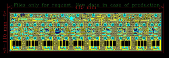
Complete PCB reverse-engineering systems integrate probing with:
7.1 Positioning Systems
- Automated XY tables with μm precision
- Vision systems for target recognition
- Force feedback for contact pressure control
7.2 Data Acquisition
- High-speed ADCs (10+ bits, 1GS/s+)
- Deep memory for capturing signal sequences
- Synchronization across multiple channels
7.3 Analysis Software
- Signal processing algorithms
- Protocol decoders
- Netlist reconstruction tools
8. Case Studies
8.1 DDR Memory Interface Probing
Challenges:
- Differential signals with tight timing
- Source-synchronous clocking
- High speeds (3200MT/s and beyond)
Solution:
- Differential probes with matched delays
- Impedance-controlled access points
- Jitter separation algorithms
8.2 Power Integrity Analysis
Challenges:
- Measuring μV-level ripple on VCC
- Wide bandwidth from DC to 100MHz+
- Low-impedance connection requirements
Solution:
- Specialized power rail probes
- Frequency-domain analysis
- Current-probing techniques
9. Future Directions
Emerging technologies in PCB probing include:
- Quantum tunneling probes: Atomic-scale resolution
- Terahertz imaging: Sub-surface trace mapping
- AI-assisted probing: Intelligent test point selection
- Self-configuring systems: Automatic probe adaptation to target characteristics
10. Conclusion
Effective probing circuits form the foundation of successful PCB reverse-engineering systems. As board technologies advance, probing systems must evolve with higher bandwidths, finer spatial resolution, and smarter signal processing capabilities. The choice between contact and non-contact methods involves tradeoffs between signal fidelity, access requirements, and potential damage to the unit under test. Future developments in materials science, MEMS technology, and signal processing algorithms will continue to push the boundaries of what’s possible in PCB analysis and reverse-engineering.
Proper implementation of probing circuits requires careful consideration of electrical characteristics, mechanical constraints, and signal integrity requirements. By understanding these fundamental principles and emerging technologies, engineers can develop more effective PCB reverse-engineering systems capable of handling tomorrow’s design challenges.