
Radio Frequency PCB Design: Principles, Materials, and Applications
Introduction
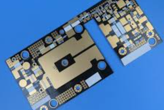
Printed Circuit Boards (PCBs) designed for Radio Frequency (RF) applications are critical components in modern wireless communication systems, radar, satellite technology, and high-speed digital circuits. Unlike conventional PCBs, RF PCBs operate at high frequencies, typically ranging from a few megahertz (MHz) to several gigahertz (GHz). Designing RF PCBs requires careful consideration of signal integrity, impedance control, material selection, and electromagnetic interference (EMI) mitigation.
This article explores the fundamentals of RF PCB design, including key principles, material selection, layout techniques, and applications in various industries.
1. Fundamentals of RF PCB Design
1.1 Frequency and Wavelength Considerations
RF signals behave differently compared to low-frequency signals due to their shorter wavelengths. At high frequencies, even small variations in trace length or impedance can cause signal reflections, attenuation, and phase distortions. The wavelength (λ) of an RF signal is given by:
[
\lambda = \frac{c}{f \sqrt{\epsilon_r}}
]
Where:
- ( c ) = Speed of light (~3 × 10⁸ m/s)
- ( f ) = Frequency of the signal
- ( \epsilon_r ) = Dielectric constant of the substrate
As frequency increases, the wavelength decreases, making the PCB layout more sensitive to parasitic effects.
1.2 Impedance Matching
Impedance matching is crucial in RF PCB design to minimize signal reflections. The characteristic impedance of transmission lines (e.g., microstrip or stripline) must match the source and load impedances (typically 50Ω or 75Ω). Mismatched impedances lead to standing waves and power loss.
Common transmission line structures in RF PCBs include:
- Microstrip: A trace on the outer layer with a ground plane beneath.
- Stripline: A trace embedded between two ground planes for better shielding.
- Coplanar Waveguide (CPW): A signal trace flanked by ground planes on the same layer.
1.3 Loss Mechanisms in RF PCBs
RF signals experience several types of losses:
- Conductor Loss: Due to the skin effect, where high-frequency currents flow near the surface of conductors, increasing resistance.
- Dielectric Loss: Caused by the substrate material’s inability to perfectly insulate, leading to energy dissipation.
- Radiation Loss: Occurs when RF energy escapes as electromagnetic waves.
2. Material Selection for RF PCBs
The choice of substrate material significantly impacts RF performance. Key properties to consider include:
2.1 Dielectric Constant (Dk or εr)
A stable dielectric constant ensures consistent impedance. Common RF materials:
- FR-4 (εr ≈ 4.3-4.8): Low-cost but lossy at high frequencies.
- Rogers RO4000 Series (εr ≈ 3.3-3.5): Low-loss, high-frequency laminates.
- PTFE (Teflon, εr ≈ 2.2-2.5): Excellent high-frequency performance but expensive.
2.2 Dissipation Factor (Df or tan δ)
A lower dissipation factor reduces dielectric losses. PTFE-based materials (Df ~0.001) outperform FR-4 (Df ~0.02).
2.3 Thermal Stability
RF circuits generate heat, requiring materials with low thermal expansion coefficients (CTE) to prevent warping.
2.4 Copper Foil Roughness
Smooth copper surfaces reduce conductor losses at high frequencies.
3. RF PCB Layout Techniques
3.1 Grounding Strategies
- Solid Ground Planes: Provide low-impedance return paths and reduce EMI.
- Via Stitching: Multiple vias connect ground layers to minimize loop inductance.
- Avoiding Ground Splits: Prevents ground loops that degrade signal integrity.
3.2 Trace Routing
- Minimize Length: Shorter traces reduce parasitic inductance and capacitance.
- Avoid Sharp Bends: Use curved or 45° angles to prevent impedance discontinuities.
- Differential Pair Routing: For high-speed signals, maintain consistent spacing and length matching.
3.3 Shielding and EMI Mitigation
- Faraday Cages: Metallic enclosures block external interference.
- Guard Traces: Grounded traces isolate sensitive RF lines from noise sources.
- Proper Filtering: Use ferrite beads and capacitors to suppress noise.
3.4 Power Delivery Network (PDN) Design
- Low-Impedance Power Planes: Reduce voltage fluctuations.
- Decoupling Capacitors: Placed near ICs to filter high-frequency noise.
4. Applications of RF PCBs
4.1 Wireless Communication
- 5G Networks: High-frequency PCBs enable millimeter-wave (mmWave) communication.
- Wi-Fi & Bluetooth: Operate at 2.4GHz and 5GHz bands.
4.2 Aerospace & Defense
- Radar Systems: RF PCBs process high-frequency signals for detection.
- Satellite Communication: Require low-loss materials for space applications.
4.3 Medical Devices
- MRI Machines: Utilize RF coils for imaging.
- Wireless Implants: Biocompatible RF PCBs for data transmission.
4.4 Automotive Radar
- ADAS (Advanced Driver Assistance Systems): 77GHz radar PCBs for collision avoidance.
5. Future Trends in RF PCB Technology
5.1 Higher Frequency Bands
With 6G and terahertz (THz) research, PCBs will need ultra-low-loss materials.
5.2 Integration with AI & IoT
Smart RF PCBs will enable real-time signal processing in IoT networks.
5.3 3D-Printed RF Circuits
Additive manufacturing may revolutionize RF PCB prototyping.
Conclusion
RF PCB design is a specialized field requiring expertise in high-frequency signal integrity, material science, and EMI control. As wireless technology advances, the demand for high-performance RF PCBs will grow, driving innovations in substrate materials, fabrication techniques, and miniaturization. Engineers must balance cost, performance, and manufacturability to meet the evolving needs of modern RF applications.
By adhering to best practices in impedance control, material selection, and layout optimization, RF PCBs can deliver reliable performance in cutting-edge communication and sensing systems.
This article provides a comprehensive overview of RF PCB design. Let me know if you’d like any sections expanded or modified!