Rigid Flex PCB Stack-up
COMMON FLEX CIRCUIT MATERIAL STACK-UP
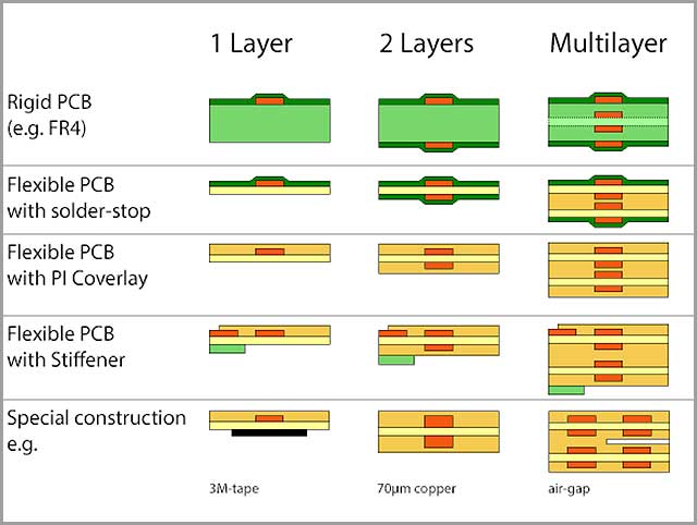
1 Layer Flex PCB with Optional FR-4 Stiffeners and PSA

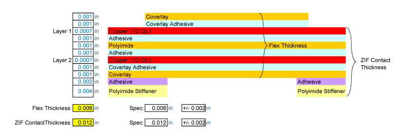
2 Layer Flex Circuit with ZIF Contact Fingers

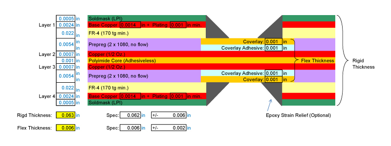
4 Layer Rigid-Flex PCB (2 Flex Layers)

The Stack Up
The stack-up is the process of placing the layers for the rigid Flex printed circuit board. Depending on the Rigid-flex circuit board, the stack-up can be of one, two, or four-layer(s), and layers increase by the object’s application as well as its uses.
Think of these layers as ingredients to a recipe, they all might be completely different from the other, yet they all combine to make for a delicious recipe, with each component adding greatness to the dish in some way, shape, or form.
The process is straightforward, but it is quite challenging to explain without a visual aid, so to explain the process better, take a look at the following diagram.

Stackup Material Information
As seen in the previous examples, the stackup contains a significant amount of information. It defines the specific material types to be used, their locations within the construction, the individual material layer thicknesses, material part numbers if required, and the total thickness of the various areas of the design.
Most flex and rigid-flex circuit designs have multiple areas with differing constructions resulting in multiple thickness requirements. Some area thicknesses may be critical to the performance of the part, either to meet a specific bend requirement, impedance value, or connector specification (ZIF connectors, for example).
For rigid-flex PCB designs, the stackup also defines the key construction elements required to meet IPC 2223C design guidelines and ensure the reliability of the finished parts.

About Andwin Circuits
Andwin Circuits as a industry leading of PCB manufacturer since 2003.
Specializing in multilayer PCB, Rigid flex PCB, HDI PCB, controlled impedance PCB and Radio Frequency circuit, from quick turn prototype to mass products.


