Thick copper PCB
Thick Copper PCB Definition
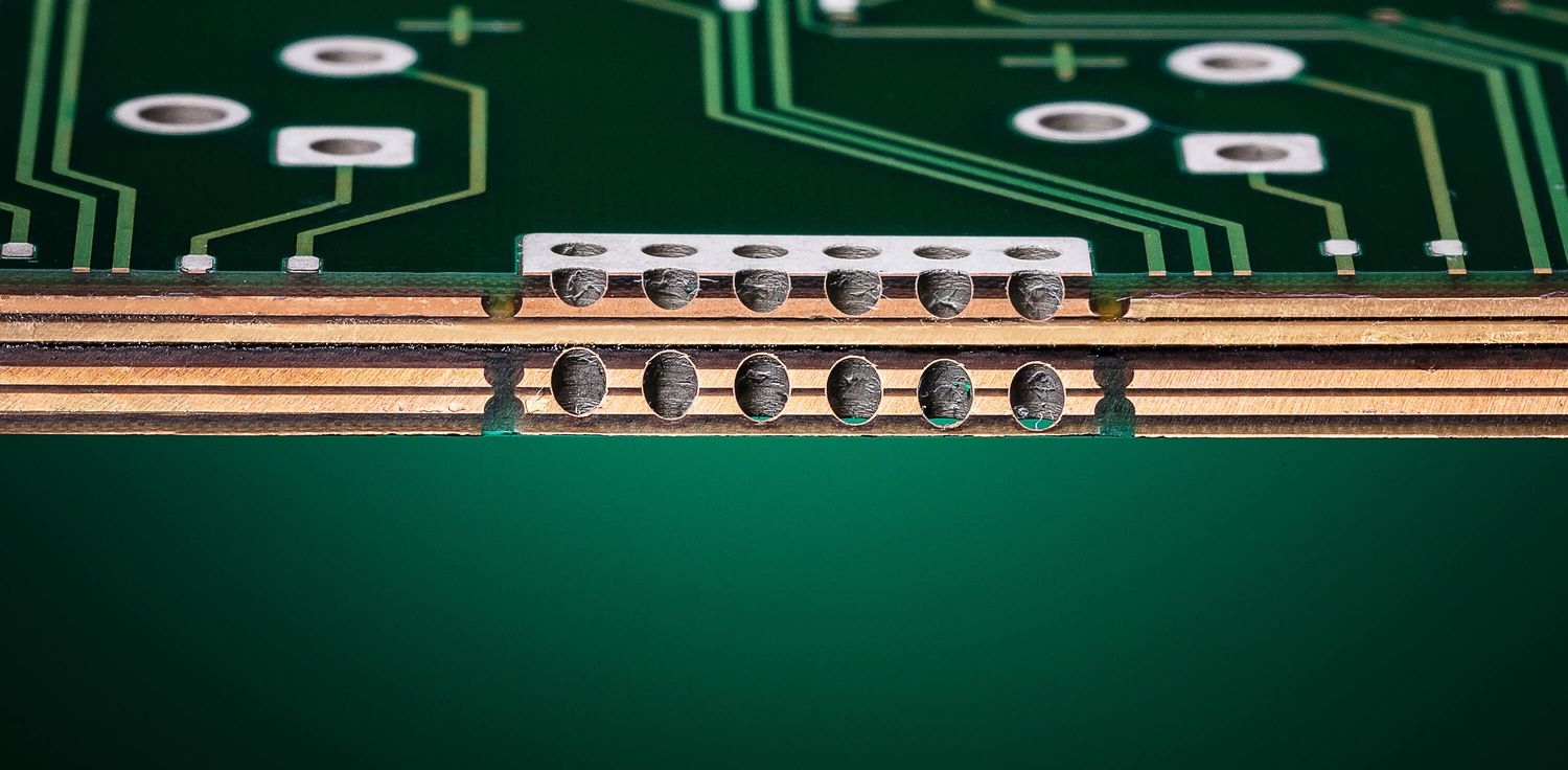
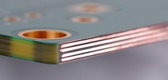
Thick Copper PCBs are printed circuit boards with 3 or more ounces of finished copper in the inner or outer layers
The additional copper PCB thickness enables the board to conduct a higher current, achieve good thermal distribution and implement complex switches in a limited space. Other advantages include increased mechanical strength at connector sites, the ability to create a smaller product size by incorporating multiple weights on the same layer of circuitry and the ability to use exotic materials to their maximum capacity with minimal risk of circuit failure.

Thick Copper PCB Manufacturing
The manufacturing processes of thick copper PCB intake the combination of multiple processes enabling extreme copper thickness requirements.
No matter single or double-sided PCBs, both need to go through the process of etching and plating.
The etching sheets of copper foil are the beginning of putting circuit layers.
Then the unwanted etched copper is removed and the plates are settled for adding thick layers of coppers to planes, traces, pads and plated-through holes.
After that, the entire circuit is being laminated into a complete package by using an epoxy-based substrate.
The PCBs are incorporated with thick copper circuits to produce specialized etching and plating techniques.
Generally, the properties are formed completely by etching thick copper-clad laminated with the board material.
This creates uneven trace sidewalls and unacceptable undercutting.
The plating technology is getting advanced that allows thick copper features to form with a combination of plating and etching.
This results in straight sidewalls and negligible undercuts.
The thick copper circuit starts to fabricate the board as soon as the thickness of copper increases the amount of copper thickness in plated holes via sidewalls.
Then it is the time when heavy copper can be mixed according to the standard feature of a single board.
Making the thick copper PCB in this way includes some advantages such as reduction of layer count,
low impedance power distribution, smaller footprints, and potential cost savings.

Generally, high-current or high-power circuits and their control circuits are produced individually for different boards.
The reason is thick copper plating makes it possible to integrate high-current circuits and
It controls the circuits to create a dense and simple board structure.
The features of thick copper connect to the seamless standard circuits to place it with minimal restriction.
It provides the designers with the ability to fabricate and discuss the manufacturing methods to make it tolerant with temperature issues.
This needs to be utilized for thick base copper to deliver a consistent and reliable high power circuit when placed in the plating and etching systems allowing the well-defined track edge within the fine lines and finer spaces.
The entire process also needs to be assured to work perfectly from prior to the final design.
Thick Copper PCB’s Capabilities
Based on the requirement, thick copper PCBs can be expensive to produce.
Thus, it is more complex in design but more effective in producing thick copper PCB.
It should have the following capabilities:
- The copper thickness up to 40 OZ ( 1400um )
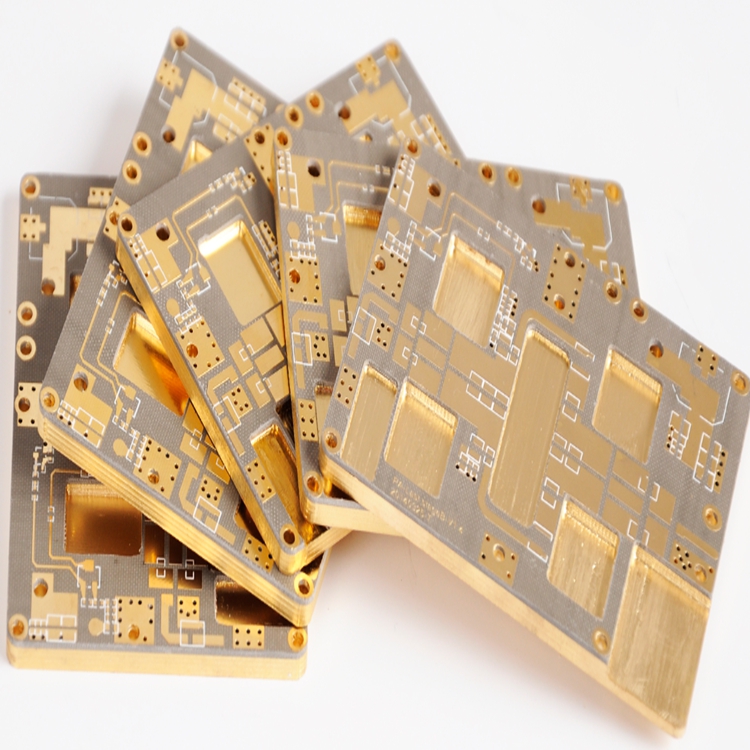
- The base material consists of FR4 / Aluminum / Copper / Ceramic
- The outline should be made of routing, punching, and V-Cut
- The solder mask comes in white, black, blue, green, or red in oil
- The surface finishing Immersion Gold, HASL and OSP
- Maximum panel size can be 580*480mm

How To Check The Thickness Of Multilayer Thick Copper PCB?
It’s generally, 2.0 ~ 3.0 mm thick. As for some small electronic products, such as electronic watches, calculators, etc. Moreover, there is no need to choose such a thick plate, 0.5 mm or thinner is enough. Similarly, the thickness of the multilayer thick copper PCB printed board is related to the number of layers.
The thickness of the multilayer board with 8 layers or less can be limited to about 1.5 mm. The thickness of more than 8 layers should exceed 1.5 mm. Thickness of each circuit layer of a multilayer board is often determined by electrical design.
Printed circuit thick copper plates are common in power supply circuits. And their electrical performance has high requirements on high voltage resistance and inductance performance, except for certain materials. Simultaneously, the particularity also has many unique points in the production.
Most of the heavy copper PCB plates by most manufacturers have a copper thickness of less than 137um. For the production of heavy copper plates with a thickness of more than 172um. The production experience is relatively lacking.

The Applications Of Thick Copper PCBs
Along with the increasing of high-power products, the demand for thick copper PCBs is greatly increased. Today’s PCB manufacturers pay more attention to using a thick copper board to solve the thermal efficiency of high-power electronics.
The thick copper PCBs are mostly large current substrate, and large current PCBs are mainly used in power module and automotive electronic parts. Traditional automotive, power supply, and power electronics applications use the original forms of transmission like cable distribution and metal sheet.
Now the heavy copper boards replace the transmission form, which not only can improve productivity and reduce the time cost of wiring, but also increase the reliability of final products. At the same time, the massive current boards can improve the design freedom of wiring, thus realizing the miniaturization of the whole product.
The following applications use heavy copper PCB :
- Power supplies and power converters
- Torque controls
- Solar power converters
- Safety and signal systems
- Power distribution
- Power line monitors
- Wielding equipment
- Rail traction systems…

With the development of new energy vehicles and intelligent driving technology, the demand for PCB will increase substantially. Moreover, pure electric and hybrid, and fuel cell vehicles require high-current thick copper PCBs. While intelligent driving radars require high-frequency (HF) PCBs.
About Andwin Circuits
Andwin Circuits as a industry leading of PCB manufacturer since 2003.
Specializing in multilayer PCB, Thick Copper PCB, Rigid flex PCB, HDI PCB, controlled impedance PCB and Radio Frequency circuit, from quick turn prototype to mass products.


