
Single-Sided vs. Double-Sided vs. Multi-Layer Flex PCBs: Which Fits Your Project?
Hardware engineering is a constant battle against physical constraints. As enclosures shrink and performance demands skyrocket, traditional rigid boards simply cannot keep up. You already know you need a flexible printed circuit, but here is the million-dollar question: should you specify a single-sided, double-sided, or multi-layer flex PCB?
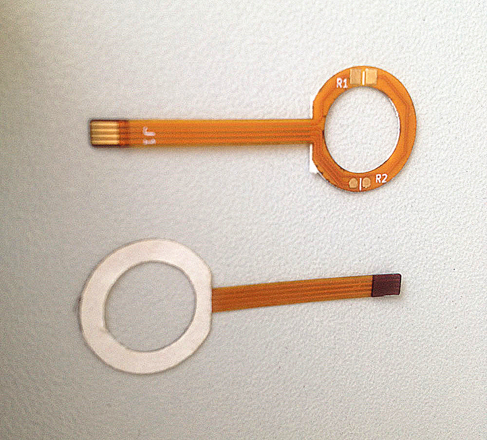
Choosing the wrong layer count doesn’t just impact your Bill of Materials (BOM) cost; it can lead to catastrophic mechanical failures, cracked copper traces, and field recalls. In this comprehensive guide, we will break down the exact engineering trade-offs between routing density, flexibility, and cost. By the end of this article, you will know exactly how to spec your next board to ensure maximum ROI and compliance with industry standards.
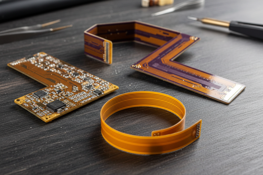
Understanding Flex PCB Layer Counts: The Basics
To understand why layer count is the most critical decision in Flex PCB manufacturing, you have to look at the core conflict in electronics design: Space vs. Complexity.
Ten years ago, a simple wearable device only needed to track steps. Today, that same device monitors heart rate, blood oxygen, GPS, and Bluetooth communications—all within a chassis that is millimeters thick. This is exactly why modern electronics increasingly using flex PCBs has become the industry standard rather than a niche exception.
However, flexibility and circuit density are inversely proportional. Every time you add a layer of copper and adhesive to route more signals, you increase the board’s stiffness. If you force a thick, multi-layer board to bend dynamically like a single-sided board, the outer copper layers will stretch beyond their tensile limits and fracture. Understanding this physical limitation is the first step to successful hardware design.
Core Concepts Simplified
Let’s strip away the marketing jargon and look at the physics of these three PCB types using plain English analogies.
Single-Sided Flex PCBs: The Champion of Dynamic Bending
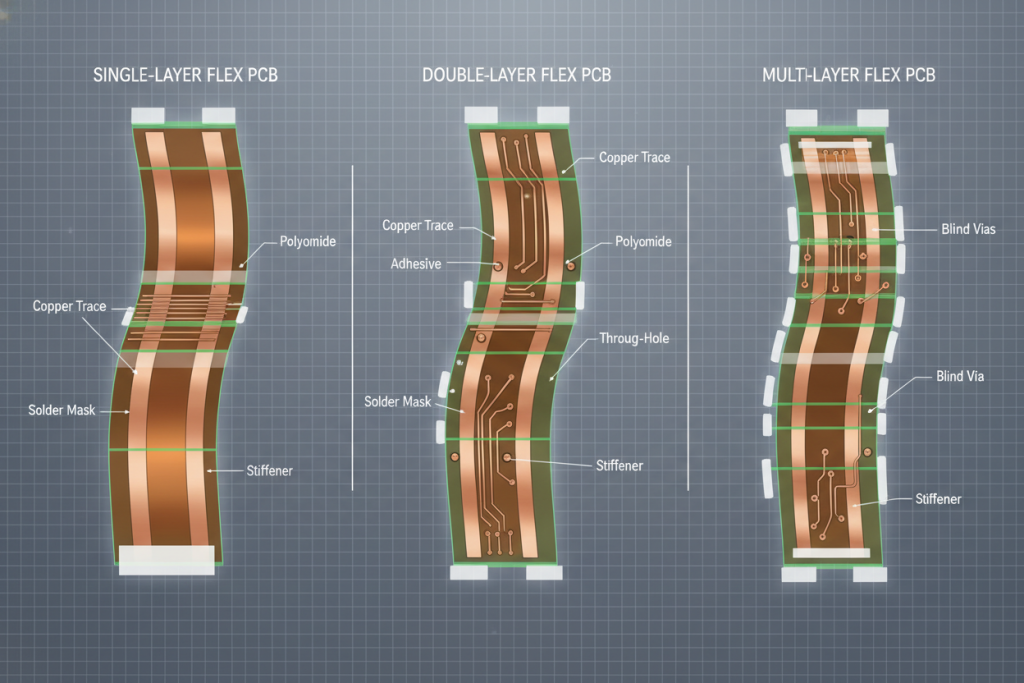
Imagine a single sheet of standard printer paper. You can fold it, roll it, and wave it back and forth thousands of times without tearing it. A single-sided flex PCB operates on the same principle. It consists of one layer of conductive copper laminated to a flexible dielectric substrate (usually Polyimide). Because there is only one copper layer, it sits perfectly on the “neutral axis” during a bend—meaning it experiences almost zero stretching or compressing forces. This is your go-to for dynamic bending (continuous movement).
Double-Sided Flex PCBs: Balancing Density and Flexibility
Now, imagine a piece of thin cardboard. It still bends, but you feel resistance, and if you crease it too sharply, the outer layer cracks. A double-sided flex PCB has two conductive layers separated by a dielectric layer. To allow electrical signals to communicate between the top and bottom layers, manufacturers drill microscopic tunnels called Plated Through Holes (PTH). You get twice the routing space, but you sacrifice extreme flexibility.
Multi-Layer Flex PCBs: Maximum Routing in Minimum Space
Think of a thick magazine. You can curve it slightly to fit it into a mailing tube, but you cannot fold it in half without ruining the spine. Multi-layer flex boards (3 to 8+ layers) are the heavyweights. They use multiple layers of copper and adhesives. They are expensive, highly complex, and relatively stiff. They are designed for static bending—meaning you bend them exactly once during factory assembly to fit them into a tight enclosure, and they never move again.
Concept Comparison Table
| Feature | Single-Sided Flex | Double-Sided Flex | Multi-Layer Flex (3+ Layers) |
|---|---|---|---|
| Copper Layers | 1 | 2 | 3 to 8+ |
| Primary Bend Type | Dynamic (Continuous motion) | Dynamic (Limited) / Static | Static (Bend-to-install only) |
| Flexibility / Lifespan | Excellent (Millions of cycles) | Good (Thousands of cycles) | Poor (Single installation fold) |
| Routing Density | Low | Medium to High | Extremely High |
| Relative Cost Multiplier | 1.0x (Baseline) | ~1.5x – 2.0x | 3.0x – 5.0x+ |
| Ideal Analogy | Sheet of paper | Thin cardboard | Thick magazine |
Step-by-Step Guide: How to Choose the Right Flex PCB
Selecting the right board is not about picking the most advanced technology; it is about matching the physical properties of the board to the mechanical reality of your product. Here is a scenario-based guide to help you make the right call.
Scenario A: High-Cycle Dynamic Bending
Your Project: A laptop hinge, a robotic arm joint, a continuous glucose monitor, or an inkjet printer head.
The Problem: The PCB must flex, twist, or roll continuously during operation.
The Solution: Single-Sided Flex PCB
When your specification sheet demands hundreds of thousands—or millions—of bend cycles, you have no other choice but single-sided flex. To ensure maximum longevity, designers must ensure the copper trace runs perpendicular to the bend line.
Engineering Tip: If you need to route a lot of signals but must maintain dynamic bending, do not add layers. Instead, increase the width of the single-sided flex board, or use multiple single-sided flex cables running parallel to each other.
Scenario B: Tight Packaging with Moderate Complexity
Your Project: A smartphone camera module, a digital SLR camera, or a compact consumer IoT device.
The Problem: You have too many components (sensors, microcontrollers) to route on one layer, but the board still needs to snake through a complex mechanical chassis.
The Solution: Double-Sided Flex PCB
Double-sided flex is the workhorse of modern consumer electronics. The addition of Plated Through Holes (PTH) allows for dense component placement (SMT) on both sides of the board. It can handle dynamic bending, but with a significantly larger minimum bend radius than single-sided boards. It is perfect for “origami-style” folding inside a device chassis.
Scenario C: Extreme Density in Unorthodox Shapes
Your Project: Aerospace avionics, advanced military hardware, or complex medical implants (like pacemakers).
The Problem: You have rigid-board levels of routing complexity (blind/buried vias, impedance control, shielding), but the final product is shaped like a cylinder or a sphere.
The Solution: Multi-Layer Flex PCB
If you are dealing with multi-layer flex, you are doing static bending (bend-to-install). The board is manufactured flat, populated with components, folded into its final 3D shape, screwed into the enclosure, and sealed. If the end-user or a technician unfolds it later, the traces will likely snap.
Flex PCB Minimum Bend Radius Specifications
To prevent trace cracking, engineers must calculate the Minimum Bend Radius based on the board’s total thickness ($T$).
| Flex PCB Type | Dynamic Bending Radius | Static Bending Radius (Install Once) | Max Recommended Layers |
|---|---|---|---|
| Single-Sided | $100 \times T$ | $6 \times T$ | 1 |
| Double-Sided | $150 \times T$ | $12 \times T$ | 2 |
| Multi-Layer | NOT RECOMMENDED | $24 \times T$ | 8+ |
(Note: $T$ = Total thickness of the flexible circuit. Always consult your manufacturer’s specific DFM guidelines).
Expert Tips & Common Pitfalls to Avoid
Even seasoned hardware engineers make mistakes when transitioning from rigid FR4 boards to flexible circuits. Here are the most common pitfalls we see on the manufacturing floor, and how to avoid them to ensure high yield rates.
Pitfall 1: Ignoring IPC-2223 Standards for Bend Areas
The most frequent cause of flex PCB failure is placing components or vias inside the bend area. According to IPC-2223 (Sectional Design Standard for Flexible Printed Boards), you must keep Plated Through Holes (PTH), surface mount components, and stiffeners strictly outside the bending zone.
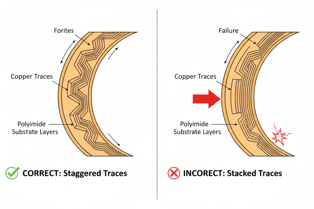
Furthermore, when routing traces through a bend area, never stack top and bottom traces directly on top of each other in a double-sided board (known as the “I-beam effect”). Instead, stagger them to distribute mechanical stress.
Pitfall 2: Selecting the Wrong Substrate Material
The layer count means nothing if your base material cannot handle the environment. While Polyimide (PI) is the gold standard for high-temperature resistance and solderability, Polyethylene Terephthalate (PET) is a cheaper alternative for low-end, low-temperature applications. If you are unsure which base material fits your BOM budget and thermal requirements, review this comprehensive PI vs PET material selection guide.
Pitfall 3: Confusing Multi-Layer Flex with Rigid-Flex
A common mistake among procurement officers is using the terms “multi-layer flex” and “rigid-flex” interchangeably. They are entirely different technologies. A multi-layer flex board is flexible throughout its entire body (even if it is stiff). A rigid-flex board actually combines standard rigid FR4 boards with flexible PI layers laminated together. If your design requires heavy components (like large BGAs or heavy connectors) combined with flexible tails, you might actually need a rigid-flex solution. To understand the cost and manufacturing variances, check out the core differences between flex and rigid PCBs.
Pitfall 4: Sharp Angles in Trace Routing
In rigid PCBs, 45-degree angles are standard. In flex PCBs, any sharp angle is a stress concentrator where copper will eventually tear during bending. Always use smooth, sweeping curves (teardrops) for trace routing, especially where traces meet solder pads.
Conclusion & Final Thoughts
Choosing between single-sided, double-sided, and multi-layer flex PCBs ultimately comes down to a strict engineering compromise: How much space do you have, and how much will the board move?
Over-engineering your board by selecting a multi-layer flex when a double-sided board would suffice will needlessly inflate your BOM costs and introduce mechanical failure risks. Conversely, trying to cram too many signals onto a single-sided board will lead to a board that is too wide for your enclosure.
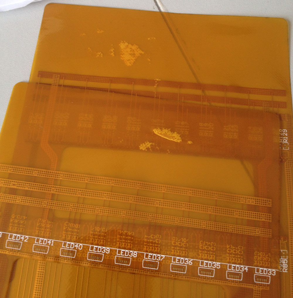
Quick Summary Matrix for Decision Makers
| Your Project Requirement | The Best Choice | Key Takeaway |
|---|---|---|
| Continuous, millions of bend cycles | Single-Sided Flex | Lowest cost, maximum lifespan, low routing density. |
| Moderate density, space-saving folds | Double-Sided Flex | The industry standard. Great balance of cost, routing (PTH), and static/light dynamic bending. |
| Extreme density, static installation | Multi-Layer Flex | High cost, stiff. Only use when complex routing (3+ layers) must fit an unorthodox 3D enclosure. |
Next Steps for Your Project:
Before you finalize your Gerber files, run a mechanical mockup using paper or thin plastic to simulate the bend radius. If you are approaching the mechanical limits of your chosen layer count, it is time to consult with a PCB manufacturing expert. Reach out to your fabrication partner for a Design for Manufacturability (DFM) check to ensure your layer stack-up aligns with IPC-2223 standards and your project’s budget.
Frequently Asked Questions
Q1: What is the key difference between single-sided and multi-layer flex PCBs?
A: Single-sided flex has one copper layer for dynamic bending; multi-layer flex has 3+ layers for extreme routing density but is strictly for static installation.
Q2: How do I choose between dynamic and static flex applications?
A: Dynamic bending requires continuous movement (use single-sided); static bending means fold once during assembly (use multi-layer).
Q3: What happens if I place vias inside the bend area?
A: It causes trace cracking and board failure. Per IPC-2223, keep all PTHs and components outside the bending zone.
Q4: Why are sharp trace angles dangerous in flex PCBs?
A: Sharp angles act as stress concentrators where copper tears during bending. Always use smooth, curved traces.
Q5: Is multi-layer flex the same as rigid-flex?
A: No. Multi-layer flex is entirely flexible; rigid-flex combines rigid FR4 sections with flexible polyimide sections.