
SMT Stencil Design: Aperture Optimization for Fine Pitch Components
Solder paste defects cause 50-70% of SMT assembly failures in high-density PCB designs, with inadequate stencil aperture design being the leading root cause. When component pitch drops below 0.5mm, stencil aperture optimization becomes critical for preventing bridging defects, insufficient solder joints, and costly production rework.
This guide covers stencil design principles, aperture optimization techniques, area ratio calculations, and component-specific strategies for fine-pitch SMT assembly. You will learn how to design stencils that achieve reliable paste deposition for 0201, 01005, QFN, and BGA packages.
What is SMT Stencil Design?
SMT stencil design is the engineering process of defining aperture dimensions, shapes, and stencil thickness to deposit precise solder paste volumes onto PCB pads during surface mount assembly. The stencil acts as a precision metering device that controls paste height, volume, and coverage for each component pad.
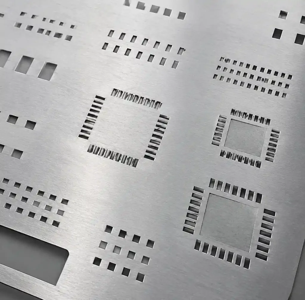
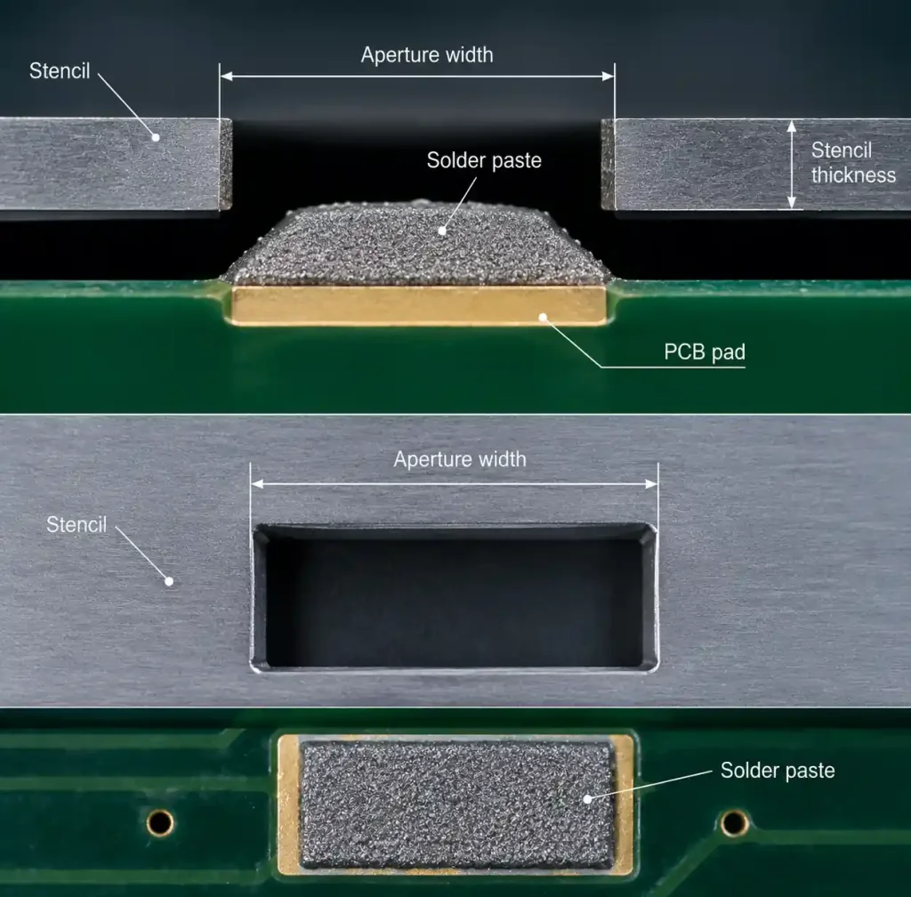
Stencil apertures are laser-cut or chemically etched openings in thin metal foil (typically stainless steel or nickel) that align with PCB solder pads. During printing, solder paste is forced through these apertures onto the board surface using a squeegee blade. Aperture dimensions directly determine paste volume, which affects solder joint formation, thermal performance, and assembly reliability.
According to IPC-7525C stencil design standards, proper aperture optimization reduces solder defects by 60-80% compared to default 1:1 pad-to-aperture designs. This becomes increasingly important as component pitch decreases and pad dimensions approach the physical limits of paste printing.
Why Aperture Optimization Matters for Fine Pitch Components
Fine pitch components with lead spacing below 0.5mm present unique challenges for solder paste printing. Standard aperture designs that work for 0.8mm pitch components often fail when applied to 0.4mm pitch QFPs or 0.3mm pitch BGAs.
Key Challenges with Fine Pitch:
- Bridging Risk: Excess paste between closely-spaced pads causes solder bridges during reflow
- Insufficient Solder: Undersized apertures deposit too little paste, creating weak or open joints
- Paste Release: Small apertures struggle to release paste cleanly from stencil walls
- Tombstoning: Uneven paste volumes on small passives cause component tilt during reflow
- Voiding: Poor aperture design for thermal pads traps flux volatiles, creating voids
Industry data shows that optimized stencil design improves first-pass yield by 15-25% for assemblies with component pitch below 0.5mm. You can achieve this improvement by applying area ratio rules, aperture reduction strategies, and component-specific modifications.
Area Ratio: The Critical Design Metric
Area ratio is the most important parameter for predicting solder paste release from stencil apertures. It is calculated as aperture area divided by aperture wall area (aperture perimeter × stencil thickness).
Area Ratio Formula:
Area Ratio = Aperture Area / (Aperture Perimeter × Stencil Thickness)IPC-7525C recommends maintaining a minimum area ratio of 0.66 for reliable paste transfer. Below this threshold, paste clings to aperture sidewalls rather than releasing cleanly onto PCB pads.
| Area Ratio | Paste Release Quality | Typical Result |
|---|---|---|
| > 0.66 | Excellent | Consistent paste deposition, minimal defects |
| 0.50 – 0.66 | Good | Acceptable with Type 3/4 paste, process optimization |
| 0.40 – 0.50 | Marginal | Requires nano-coating, controlled environment |
| < 0.40 | Poor | Inconsistent release, high defect rates |
For 01005 components (0.4mm × 0.2mm pads), achieving 0.66 area ratio requires either reducing stencil thickness to 75-100μm or using alternative aperture shapes. Many high-volume manufacturers successfully operate at 0.45-0.50 area ratio with Type 3 solder paste and nano-coated stencils.
Stencil Thickness Selection
Stencil thickness directly affects both paste volume and area ratio. Thicker stencils deposit more paste but reduce area ratio for small apertures. You must balance adequate solder volume against reliable paste release.
| Application | Recommended Thickness | Component Types |
|---|---|---|
| Ultra-Fine Pitch | 75-100μm (3-4 mil) | 01005, 0201, 0.3mm pitch BGA |
| Fine Pitch | 100-125μm (4-5 mil) | 0402, 0.5mm pitch QFN/QFP |
| Standard SMT | 125-150μm (5-6 mil) | 0603, 0805, SOIC, standard pitch |
| High Power | 150-200μm (6-8 mil) | Large discretes, power components |
For mixed assemblies with both fine-pitch ICs and larger discretes, step stencils provide localized thickness variations. The stencil is thinner in fine-pitch regions (100μm) and thicker for high-power components (150μm), optimizing area ratio across the entire board.
Andwin Circuits recommends 100-125μm thickness for most fine-pitch assemblies, achieving the right balance between paste volume and printability for components down to 0.4mm pitch.
Aperture-to-Pad Sizing Guidelines
Aperture dimensions should be slightly smaller than PCB pad dimensions to prevent excess paste that causes bridging. The reduction percentage depends on component type, pitch, and pad geometry.
Standard Aperture Reduction:
- Fine Pitch IC Leads (≤0.5mm pitch): 10-15% reduction in width and length
- QFN Perimeter Pads: 10% reduction, maintains thermal pad at 1:1 or custom pattern
- BGA Pads (≥0.5mm): 5-10% reduction for non-solder mask defined pads
- 0201/01005 Passives: 5% reduction in length, 0-5% in width
- Standard Passives (≥0402): 1:1 aperture-to-pad ratio typically acceptable
For 0.5mm pitch QFP with 0.25mm × 1.5mm pads, you would design apertures at 0.22mm × 1.35mm (12% × 10% reduction). This provides sufficient paste while maintaining 0.03mm clearance between adjacent paste deposits.
Aperture Optimization for Specific Components
0201 and 01005 Passive Components
Ultra-small passive components require careful aperture design to prevent tombstoning and ensure adequate solder fillet formation.
0201 Component (0.6mm × 0.3mm):
- Stencil thickness: 100μm (4 mil)
- Aperture size: 0.55mm × 0.28mm (8% × 7% reduction)
- Area ratio: 0.50-0.55
- Solder paste: Type 3 or Type 4
01005 Component (0.4mm × 0.2mm):
- Stencil thickness: 75-100μm (3-4 mil)
- Aperture size: 0.38mm × 0.19mm (5% × 5% reduction)
- Area ratio: 0.40-0.48
- Solder paste: Type 4 required
At these dimensions, you approach the practical limits of stencil printing. Nano-coated stencils improve paste release for area ratios below 0.50, extending the viable printing window for 01005 assemblies.
QFN and DFN Package Thermal Pads
Quad Flat No-lead (QFN) packages feature large center thermal pads that require special aperture treatment to prevent voiding while maintaining adequate paste volume.
Thermal Pad Aperture Strategies:
- Window Pane Pattern: Divide large pad into 4-9 smaller apertures with gaps for flux escape
- Cross-Hatch Pattern: Grid of apertures covering 50-70% of pad area
- Border Frame: Aperture around pad perimeter with center gap
- Solid Reduced: Single aperture at 80-90% of pad size
For a 5mm × 5mm QFN thermal pad, a 3×3 window pane pattern with 1.5mm square apertures and 0.5mm gaps provides 65% paste coverage. This allows flux volatiles to escape during reflow, reducing void percentage from 25-40% (solid aperture) to 5-15% (window pane).
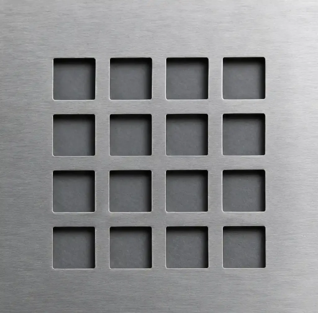
QFN perimeter leads require 10% aperture reduction to prevent bridging at 0.5mm pitch. Step stencils are often used, with 100μm thickness for perimeter leads and 125-150μm for the thermal pad region.
Fine Pitch BGA and CSP
Ball Grid Array packages with pitch below 0.5mm demand precise aperture control to prevent bridging while maintaining adequate solder volume for reliable ball attachment.
BGA Aperture Guidelines:
| BGA Pitch | Pad Size | Aperture Size | Stencil Thickness | Area Ratio |
|---|---|---|---|---|
| 0.8mm | 0.45mm | 0.40-0.42mm | 125μm | 0.76-0.80 |
| 0.65mm | 0.35mm | 0.32-0.33mm | 100μm | 0.74-0.79 |
| 0.5mm | 0.27mm | 0.24-0.25mm | 100μm | 0.60-0.65 |
| 0.4mm | 0.20mm | 0.18-0.19mm | 75μm | 0.55-0.63 |
| 0.3mm | 0.15mm | 0.13-0.14mm | 75μm | 0.42-0.48 |
For 0.4mm pitch BGAs, circular apertures slightly undersized from pads provide the best results. At 0.3mm pitch, you enter the marginal printing zone where area ratio drops below 0.50 and process control becomes critical.
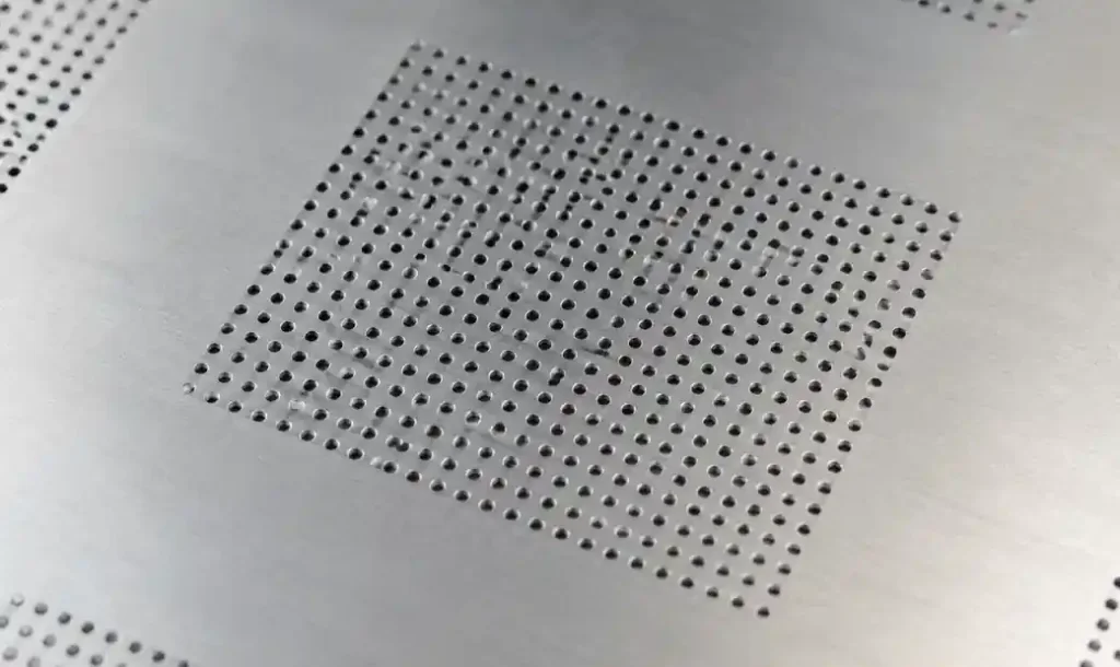
Andwin Circuits successfully manufactures assemblies with BGA pitch down to 0.3mm using 75μm laser-cut stencils, Type 4 solder paste, and controlled printing parameters (print speed 20-30mm/s, squeegee pressure 0.3-0.5 kg/cm, humidity 45-55% RH).
Fine Pitch QFP and TSSOP
Quad Flat Pack and Thin Shrink Small Outline Package components with lead pitch below 0.5mm require elongated aperture reductions to prevent bridging.
For 0.4mm pitch QFP with 0.18mm × 1.2mm pads:
- Aperture width: 0.16mm (11% reduction)
- Aperture length: 1.08mm (10% reduction)
- Stencil thickness: 100μm
- Area ratio: 0.53
The width reduction is more aggressive than length reduction because bridging risk is highest in the cross-pitch direction. Maintaining 0.02mm paste-free gap between adjacent deposits prevents solder bridges during reflow.
Step Stencil Technology
Step stencils (also called multi-level or graduated stencils) incorporate multiple thickness regions in a single stencil, optimizing paste deposition for mixed-component assemblies.
When to Specify Step Stencils:
- Mix of 0201/0402 components with QFN thermal pads
- Fine-pitch ICs (0.4-0.5mm) alongside standard pitch components
- Connector pins requiring high paste volume next to fine-pitch BGAs
- LED assemblies with both small-signal ICs and high-power LEDs
Step stencils are manufactured by secondary etching or electroforming processes that create thickness transitions between board regions. Typical configurations include 100μm for fine-pitch areas and 150μm for standard components.
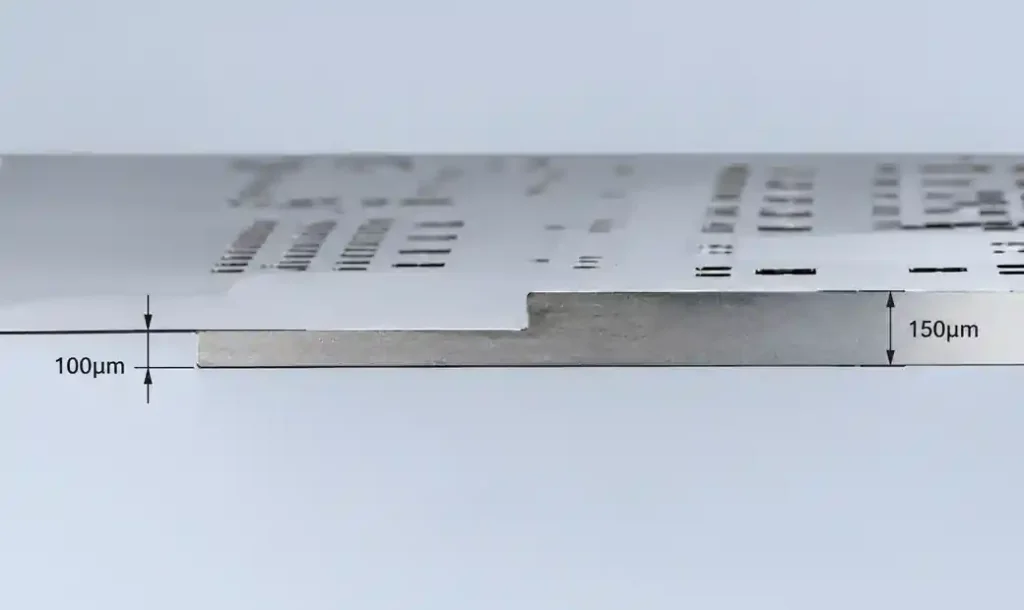
The thickness transition should occur in non-critical areas, avoiding apertures in the step region. Cost premium for step stencils is 40-60% over standard stencils, justified when alternative approaches (separate stencils, manual paste dispensing) are impractical.
Aperture Shape Modifications
Beyond dimensional reductions, aperture shape modifications improve paste deposition for specific geometries.
Home Plate Aperture: For rectangular pads, angled corners on the squeegee-trailing edge improve paste release by reducing the last point of contact area. This technique works best for pads with aspect ratios above 3:1.
Rounded Apertures: Circular or rounded-corner apertures provide better paste release than sharp corners for small pads. The reduced perimeter-to-area ratio improves area ratio by 5-10%.
Elongated Reductions: For closely-spaced IC leads, reducing aperture width more than length maintains paste volume while creating adequate paste-free gaps between adjacent pads.
Nano-Coating and Surface Treatment
Nano-coating applies a thin (200-500nm) fluoropolymer or ceramic layer to stencil surfaces, reducing surface energy and improving paste release characteristics. This technology extends the workable area ratio down to approximately 0.40.
Benefits of Nano-Coated Stencils:
- Improved paste release for area ratios of 0.40-0.50
- Extended stencil life (3-5× longer between cleanings)
- Better performance with lead-free solder pastes
- Reduced stringing and bridging defects
- Lower squeegee pressure requirements
Nano-coating adds 30-50% to stencil cost but significantly improves yields for ultra-fine-pitch assemblies. The coating wears over time and typically requires reapplication after 50,000-100,000 print cycles.
Andwin Circuits uses nano-coated stencils for all assemblies with component pitch below 0.4mm or area ratios below 0.55, improving first-pass yield by 12-18% compared to standard stencil surfaces.
Design Verification and First Article Testing
Before committing to production volumes, stencil designs should be validated through first article testing that measures paste deposition performance.
Stencil Validation Process:
- CAD Review: Verify aperture dimensions match design calculations
- Laser Measurement: Confirm aperture sizes within ±10μm tolerance
- Solder Paste Inspection (SPI): Measure deposited paste volume, height, and area
- Reflow Analysis: Inspect for bridging, insufficient solder, voiding
- X-Ray Inspection: Verify BGA and QFN solder joint formation
SPI data should show paste volume within 80-150% of aperture volume (accounting for transfer efficiency). Heights should be consistent within ±10% across repeated prints. Any apertures consistently outside this window require modification before production release.
IPC-7525C Design Standards
IPC-7525C is the industry standard for stencil design, providing guidelines for aperture dimensions, aspect ratios, and process parameters.
Key IPC-7525C Requirements:
- Aspect Ratio (minimum): 1.5 (width / thickness), preferably 1.7+
- Area Ratio (minimum): 0.66 for reliable printing
- Aperture Tolerance: ±25μm (±1 mil) for laser-cut stencils
- Surface Finish: Ra < 0.5μm for nano-coated, Ra < 1.0μm standard
- Alignment Accuracy: ±25μm registration to PCB pads
Following IPC-7525C guidelines ensures stencil designs meet industry-accepted reliability standards for high-volume manufacturing. Andwin Circuits designs all stencils per IPC-7525C and validates performance through SPI and first article inspection.

Common Stencil Design Mistakes
Mistake 1: Using 1:1 Aperture-to-Pad Ratio for Fine Pitch
For pitch below 0.5mm, 1:1 ratios deposit excess paste that causes bridging. Apply 10-15% reductions based on component type.
Mistake 2: Ignoring Area Ratio Calculations
Small apertures with thick stencils create area ratios below 0.50, leading to inconsistent paste release and high defect rates.
Mistake 3: Solid Apertures for Large Thermal Pads
QFN thermal pads require window pane or cross-hatch patterns to allow flux escape during reflow, reducing void formation.
Mistake 4: Mixing Fine-Pitch and High-Power Components on Single-Thickness Stencil
Step stencils optimize paste volume across different component types, improving overall yield.
Mistake 5: No First Article Validation
Proceeding to production without SPI verification of paste deposition leads to costly rework and schedule delays.
Conclusion
Optimized stencil aperture design is critical for reliable SMT assembly of fine-pitch components. By applying area ratio calculations, component-specific aperture modifications, and IPC-7525C design standards, you can achieve consistent solder paste deposition for components down to 0.3mm pitch.
The key principles are maintaining area ratios above 0.50, reducing apertures 10-15% for fine-pitch leads, using window pane patterns for thermal pads, and validating designs through SPI before production. Step stencils and nano-coating extend the workable design space for mixed assemblies and ultra-fine-pitch components.
If you need high-quality PCB assembly with optimized stencil design for fine-pitch components, Andwin Circuits offers advanced SMT capabilities including 01005 component assembly, 0.3mm pitch BGA placement, and X-ray inspection for QFN packages. Our facility is certified to IPC-A-610 Class 3 and ISO 9001, ensuring superior quality for your electronic products.
Contact us today for turnkey PCB assembly, stencil design optimization, and fast delivery in 7 days.
FAQ
What is the minimum area ratio for reliable solder paste printing?
IPC-7525C recommends a minimum area ratio of 0.66 for reliable paste transfer. For fine-pitch components, area ratios of 0.50-0.66 can work with Type 3/4 solder paste and optimized printing parameters. Below 0.40, paste release becomes inconsistent and defect rates increase significantly.
What stencil thickness should I use for 0201 and 01005 components?
For 0201 components, use 100μm (4 mil) stencil thickness. For 01005, reduce to 75-100μm (3-4 mil) to improve area ratio. Thinner stencils improve paste release but require Type 4 solder paste and controlled printing parameters.
How much should I reduce apertures for fine-pitch IC leads?
For component pitch below 0.5mm, reduce aperture dimensions by 10-15% compared to PCB pads. Width reduction is typically more aggressive than length reduction to prevent bridging between adjacent leads.
What aperture pattern works best for QFN thermal pads?
Window pane patterns with 50-70% paste coverage provide the best balance between thermal performance and void reduction. For a 5mm × 5mm thermal pad, use a 3×3 grid of 1.5mm apertures with 0.5mm gaps for flux escape.
Can I use standard stencils for 0.3mm pitch BGA?
0.3mm pitch BGAs require 75μm laser-cut stencils with nano-coating for reliable printing. Area ratios fall to 0.42-0.48, making process control critical. Type 4 solder paste, controlled humidity (45-55% RH), and SPI verification are necessary for consistent results.
What is the cost difference between standard and step stencils?
Step stencils cost 40-60% more than standard single-thickness stencils due to additional manufacturing steps. The cost is justified for mixed assemblies where fine-pitch and high-power components cannot be optimized with a single thickness.
How often should stencils be replaced in high-volume production?
Standard stencils last 100,000-200,000 print cycles before aperture dimensions drift outside tolerance. Nano-coated stencils extend life by reducing paste buildup and aperture wear. Monitor paste deposition via SPI and replace stencils when volume consistency degrades.
What solder paste type works best for fine-pitch assemblies?
Type 3 solder paste (25-45μm particle size) works well for pitch down to 0.4mm. For 0.3mm pitch and 01005 components, Type 4 paste (20-38μm particles) provides better printability through small apertures. Type 5 (15-25μm) is rarely needed and has reduced wetting properties.