
Skip to content
Andwin Circuits
  • Home
  • ProductsExpand
    • HDI multilayer PCB
    • Rigid Flex PCB
    • Flex pcb
    • Special PCBExpand
      • High Frequency PCBExpand
        • Rogers RO4350B PCB
        • Rogers RO4003 pcb
        • Rogers RO3003 PCB
        • Rogers 5880 PCB
        • DICLAD 527 PCB
        • Taconic TLX series
        • Taconic TLX-8 RF PCB
        • Taconic TLX-9 RF PCB
      • High speed pcbExpand
        • Megtron 6 High Speed PCB
        • TU-872 SLK Sp High Speed
      • High TG PCBExpand
        • SHENGYI SH260 PCB
        • ISOLA 370HR PCB
        • ISOLA IS410 PCB
        • ISOLA IS420 PCB
      • Heavy copper PCB
      • Copper coin pcb
      • Copper inlay PCB
    • Metal Core PCBExpand
      • Copper core pcb
      • Aluminum PCB
      • 2 Layers Aluminum PCB
      • Direct thermal MCPCB
      • 2 Layers Direct Thermal
    • Ceramic PCBExpand
      • DPC ceramic PCB
      • DBC ceramic PCB
      • Thick film Ceramic PCB
      • Al2O3 Alumina PCB
      • AIN ALN ceramic PCB
      • IGBT Ceramic PCB
  • ServiceExpand
    • PCB Assembly
    • Quick turn PCB assembly
    • PCBA conformal coating
  • IndustryExpand
    • Telecommunication
    • IoT and Wireless
    • Industrial Control
    • Thermal management
    • Power and Energy
    • IC test board
    • Automative
    • Medical
  • CapabilityExpand
    • Rigid PCB
    • Rigid flex PCB
    • Metal core PCB
    • PCB Assembly
  • TechnologyExpand
    • Blogs
    • Via in pad
    • PCB E-test
    • PCB stack up
    • MCPCB panelization
    • Controlled impedance PCB
  • AboutExpand
    • About us
    • Certification
    • Factory Tour
  • Contact
Andwin Circuits
Home / Summary of 8 common PCB markings

Summary of 8 common PCB markings

ByGrace May 9, 2025May 8, 2025

Today I will share with you: 8 common PCB markings on PCB boards.

From left to right: stamp hole – via type – solder mask pad – fiducial mark

From left to right: PCB slot, PCB button, spark gap and fuse trace

1.PCB stamp hole
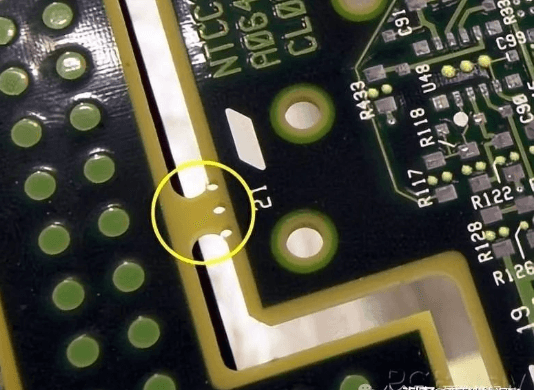
    Stamp hole

    When assembling boards, in order to facilitate the separation of PCB boards, a small contact area is reserved in the middle, and the hole in the area is called a stamp hole. I personally think that the reason for the name stamp hole is that when the PCB is separated, it leaves an edge like a stamp.

    2.PCB via type
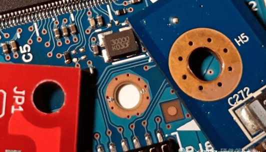
      PCB via type

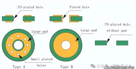
      In many cases, you will see mounting holes surrounded by tiny vias. There are mainly 2 types of mounting holes here: plated and unplated. There may be 2 reasons to use surrounding vias:

      1. When we want to connect the hole with the inner layer (such as GND in multi-layer PCB)
      2. In the case of unplated holes, when you want to connect the upper and lower pads
      3.Solder mask pad (solder stealing)
      One of the defects of wave soldering is that solder bridges are prone to occur during soldering of SMD. As a solution, people found that using extra pads at the end of the original pins can solve the problem. The width of the extra pad is 2-3 times that of the normal pad.

        Also known as solder stealing, because excess solder is absorbed and solder bridges are prevented.

        Solder mask pad

        4.Fiducial Mark (Mark Point Mark)
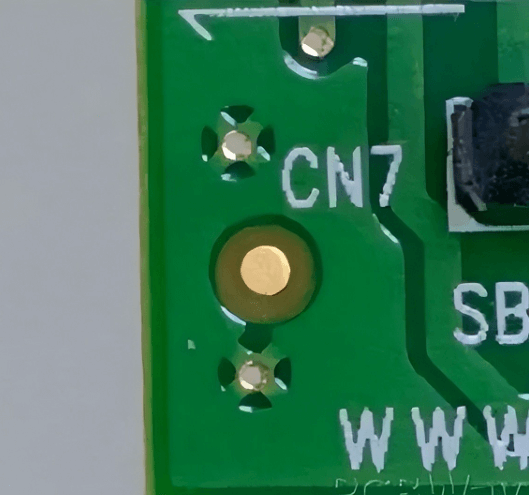
          Fiducial Mark

          There is a bare copper circle inside a larger bare circle. This fiducial mark is used as a reference point for the pick and place (PnP) machine. The fiducial mark is located in three locations:

          1. In the panel.
          2. Except for small pitch parts such as QFN, TQFP.
          3. At the corners of the PCB.

          For more details about the fiducial mark, please read the following article:

          How to make a mark? 9 mark positioning principles, pictures and examples, to help you get the mark

          5.Spark gap


          Spark gaps are used for ESD, current surge and overvoltage protection. High voltage ionizes the air between the two terminals and forms a spark between them before damaging the rest of the circuit. This type of protection is not recommended, but it is better than nothing. The main disadvantage is that the performance will change over time.

            The breakdown voltage can be calculated by the following formula: V=((3000×p×d)+1350)

            Where “p” is the atmospheric pressure and “d” is the distance in millimeters.
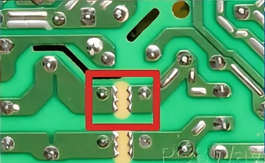
            Spark gap

            6.PCB conductive key

            If you have disassembled a remote control or calculator, you should have seen this mark. The conductive key consists of 2 staggered terminals (but not connected). When the rubber button on the keyboard is pressed, the two terminals are connected because the bottom of the rubber button is conductive.
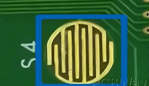
            PCB Conductive Buttons

            7.Fuse Tracking


            Similar to spark gaps, this is another cheap technique using PCBs. Fuse tracks are necked tracks on power lines and are one-time fuses. The same configuration can be used as a PCB jumper to remove a specific connection by simply etching the necked trace (PCB jumpers can be found on the reset line on some Arduino UNO boards).
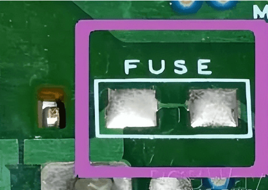
              Fuse Tracking

              8.PCB Slotting

              If you look at a high-voltage device PCB such as a power supply, you may notice that there are air slots between some of the traces.

                Repeated temporary arcs in the PCB can cause the PCB to carbonize, resulting in a short circuit. To do this, wiring slots can be added to the suspected area, where arcs will still occur but will not carbonize.
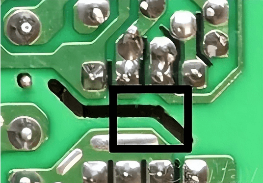
                PCB Slots

                Contact us for PCB quote now |
                Post Tags: #aluminum clad pcb#aluminum core pcb#aluminum pcb#pcb marking

                Post navigation

                Previous Previous
                Precision Techniques in Surface Mount PCB Assembly Optimization
                NextContinue
                Don’t get confused anymore! Teach you to distinguish through holes, blind holes, and buried holes in PCBs!

                Search

                Search

                Products

                • HDI Multilayer PCB
                • Rigid Flex PCB
                • Flex pcb
                • High Frequency PCB
                • High speed pcb
                • Heavy copper PCB
                • Metal Core PCB
                • Ceramic PCB

                Address

                Andwin Circuits Co.,Limited
                Email: sales@andwinpcb.com
                Tel: +86 755 2832 9394
                Fax:+86 755 2992  6717
                ADD:1-2F-1217,HouDeQun Industrial park,
                NanTing RD NO.56,ShaJing,BaoAn,Shenzhen 518104,GuangDong,China

                Products

                • HDI Multilayer PCB
                • Rigid Flex PCB
                • Flex pcb
                • High Frequency PCB
                • High speed pcb
                • Heavy copper PCB
                • Metal Core PCB
                • Ceramic PCB

                Technology

                • Blogs
                • Via in pad
                • PCB E-test
                • PCB stack up
                • Metal core PCB panelization
                • Controlled impedance PCB

                CERTIFICATION

                Certification >>


                Copyright© 2003 - 2026 Andwin | All Rights Reserved | Powered by Andwin

                Scroll to top
                • Home
                • Products
                  • HDI multilayer PCB
                  • Rigid Flex PCB
                  • Flex pcb
                  • Special PCB
                    • High Frequency PCB
                      • Rogers RO4350B PCB
                      • Rogers RO4003 pcb
                      • Rogers RO3003 PCB
                      • Rogers 5880 PCB
                      • DICLAD 527 PCB
                      • Taconic TLX series
                      • Taconic TLX-8 RF PCB
                      • Taconic TLX-9 RF PCB
                    • High speed pcb
                      • Megtron 6 High Speed PCB
                      • TU-872 SLK Sp High Speed
                    • High TG PCB
                      • SHENGYI SH260 PCB
                      • ISOLA 370HR PCB
                      • ISOLA IS410 PCB
                      • ISOLA IS420 PCB
                    • Heavy copper PCB
                    • Copper coin pcb
                    • Copper inlay PCB
                  • Metal Core PCB
                    • Copper core pcb
                    • Aluminum PCB
                    • 2 Layers Aluminum PCB
                    • Direct thermal MCPCB
                    • 2 Layers Direct Thermal
                  • Ceramic PCB
                    • DPC ceramic PCB
                    • DBC ceramic PCB
                    • Thick film Ceramic PCB
                    • Al2O3 Alumina PCB
                    • AIN ALN ceramic PCB
                    • IGBT Ceramic PCB
                • Service
                  • PCB Assembly
                  • Quick turn PCB assembly
                  • PCBA conformal coating
                • Industry
                  • Telecommunication
                  • IoT and Wireless
                  • Industrial Control
                  • Thermal management
                  • Power and Energy
                  • IC test board
                  • Automative
                  • Medical
                • Capability
                  • Rigid PCB
                  • Rigid flex PCB
                  • Metal core PCB
                  • PCB Assembly
                • Technology
                  • Blogs
                  • Via in pad
                  • PCB E-test
                  • PCB stack up
                  • MCPCB panelization
                  • Controlled impedance PCB
                • About
                  • About us
                  • Certification
                  • Factory Tour
                • Contact
                Search