Surface Mount Stencil: A Comprehensive Guide
Introduction
Surface Mount Technology (SMT) has revolutionized the electronics manufacturing industry by enabling the production of smaller, faster, and more efficient printed circuit boards (PCBs). A critical component in the SMT assembly process is the surface mount stencil, also known as an SMT stencil or solder paste stencil. This thin sheet, typically made of stainless steel or other materials, is used to deposit precise amounts of solder paste onto PCB pads before component placement.
This article explores the fundamentals of surface mount stencils, including their types, materials, manufacturing processes, design considerations, and best practices for optimal performance in SMT assembly.
1. What is a Surface Mount Stencil?
A surface mount stencil is a precision tool with laser-cut openings that correspond to the solder pad locations on a PCB. When solder paste is applied over the stencil using a squeegee, it passes through the apertures and deposits onto the PCB pads. This ensures accurate and consistent solder paste application, which is crucial for reliable solder joints during reflow soldering.
Key Functions of an SMT Stencil:
- Precise solder paste deposition – Ensures the right amount of paste is applied to each pad.
- Consistency in volume and shape – Maintains uniform solder joints across the PCB.
- High-speed printing – Facilitates rapid assembly in high-volume production.
- Minimizes defects – Reduces issues like bridging, insufficient solder, or misalignment.
2. Types of Surface Mount Stencils
Surface mount stencils come in different types based on material, construction, and application requirements.
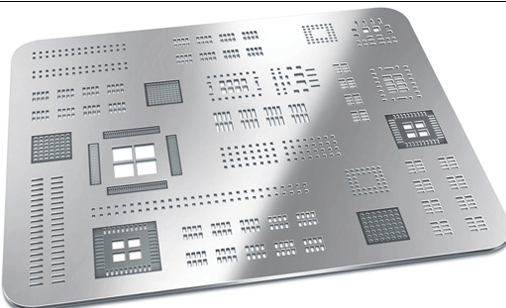
A. Framed Stencils
- Permanently mounted on a metal frame (usually aluminum).
- Used in automated solder paste printers.
- Provides high stability and repeatability.
- Ideal for high-volume production.
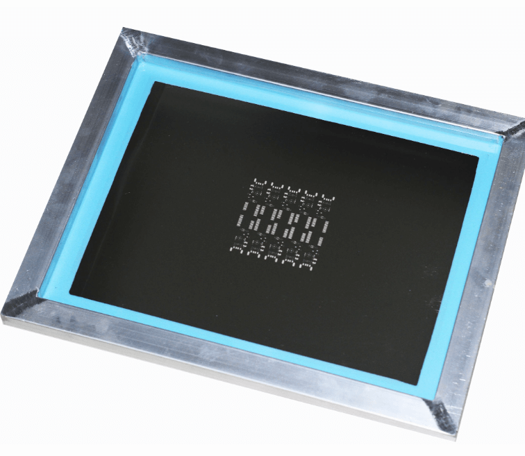
B. Frameless Stencils
- No permanent frame; held in place by a reusable tensioning system.
- Lower cost and easier storage.
- Suitable for prototyping and low-to-medium volume production.
C. Step Stencils
- Feature varying thicknesses to accommodate different component sizes.
- Used when a single PCB has mixed components (e.g., fine-pitch ICs and large connectors).
- Improves solder paste release for both small and large apertures.
D. Nano-Coated Stencils
- Coated with a non-stick material (e.g., nickel or polymer) to reduce solder paste sticking.
- Enhances paste release and reduces cleaning frequency.
- Ideal for ultra-fine-pitch components.
E. Electroformed Stencils
- Made through an electroforming process for ultra-precise apertures.
- Excellent for micro-BGA and 01005 components.
- High durability but more expensive than laser-cut stencils.
3. Materials Used in SMT Stencils
The choice of material affects stencil durability, performance, and cost.
| Material | Pros | Cons | Best For |
|---|---|---|---|
| Stainless Steel | Durable, cost-effective, good paste release | May wear over time | Most SMT applications |
| Nickel | Longer lifespan, smoother aperture walls | Higher cost | High-volume production |
| Polyimide (Plastic) | Flexible, low cost | Less durable, poor for fine-pitch | Prototyping, low-volume |
| Electroformed Nickel | Ultra-precise apertures | Expensive, longer lead time | Micro-BGA, 01005 components |
4. Manufacturing Processes for SMT Stencils
The manufacturing method influences stencil precision and performance.
A. Laser Cutting
- Most common method.
- Uses a high-power laser to cut apertures.
- High precision (±10µm accuracy).
- Suitable for most SMT applications.
B. Chemical Etching
- Uses acid to etch apertures.
- Lower cost but less precise than laser cutting.
- Limited to stencils thicker than 100µm.
C. Electroforming
- Builds nickel stencils layer by layer.
- Extremely precise (down to 15µm).
- Used for ultra-fine-pitch components.
D. Hybrid Stencils
- Combines laser cutting and electroforming.
- Optimized for mixed-technology PCBs.
5. Key Design Considerations for SMT Stencils
Proper stencil design is crucial for high-quality solder paste deposition.
A. Aperture Design
- Aperture Size: Should match PCB pad dimensions (typically 1:1 for standard components).
- Aperture Shape: Rectangular for most components, home-shaped for improved paste release.
- Aspect Ratio (Aperture Width / Thickness): Should be ≥1.5 for good paste transfer.
- Area Ratio (Aperture Area / Wall Area): Should be ≥0.66 to prevent clogging.
B. Stencil Thickness
- Standard Components: 100-150µm.
- Fine-Pitch Components (0.4mm pitch or less): 80-100µm.
- Large Components (QFN, connectors): 150-200µm (or step stencil).
C. Stencil Coatings
- Nano-coatings improve paste release.
- Anti-wear coatings extend stencil life.
D. Fiducial Marks & Alignment
- Ensure proper stencil-to-PCB alignment.
- Critical for fine-pitch and BGA components.
6. Best Practices for Using SMT Stencils
To maximize stencil performance and PCB assembly quality:
- Regular Cleaning – Prevent solder paste buildup using wipes or automated cleaners.
- Proper Storage – Store stencils flat or in protective cases to avoid warping.
- Squeegee Selection – Use metal or polyurethane squeegees at 45-60° angles.
- Print Pressure & Speed – Optimize for consistent paste deposition.
- Inspection & Maintenance – Check for wear, damage, or aperture clogging.
7. Common Defects & Troubleshooting
| Defect | Cause | Solution |
|---|---|---|
| Insufficient Solder | Aperture too small, poor release | Increase aperture size, use nano-coating |
| Solder Bridging | Too much paste, stencil misalignment | Reduce stencil thickness, improve alignment |
| Paste Smearing | Dirty stencil, excessive pressure | Clean stencil, adjust squeegee pressure |
| Clogged Apertures | Dried paste, poor cleaning | Frequent cleaning, use smaller aperture designs |
8. Future Trends in SMT Stencil Technology
- 3D Printed Stencils – For rapid prototyping and custom designs.
- Smart Stencils – Embedded sensors for real-time process monitoring.
- AI-Optimized Designs – Machine learning for aperture optimization.
- Eco-Friendly Materials – Sustainable stencil materials with longer lifespans.
Conclusion
Surface mount stencils play a vital role in ensuring high-quality solder paste deposition, which directly impacts PCB assembly reliability. By understanding stencil types, materials, design principles, and best practices, manufacturers can optimize their SMT processes for efficiency and defect-free production. As technology advances, innovations in stencil manufacturing and materials will continue to push the boundaries of precision and performance in electronics manufacturing.
By leveraging the right stencil solutions, companies can achieve higher yields, reduced rework, and improved product quality in their SMT assembly lines.