Optimizing HDI PCB Layouts for Maximum Density
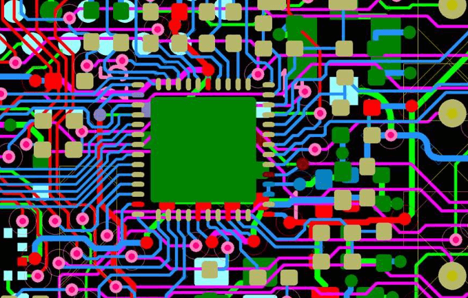
“Master HDI PCB design optimization with micro via placement, trace width reduction, and IPC-2226 compliance strategies for ultra-compact layouts using advanced EDA tools like Altium Designer.”

“Master HDI PCB design optimization with micro via placement, trace width reduction, and IPC-2226 compliance strategies for ultra-compact layouts using advanced EDA tools like Altium Designer.”
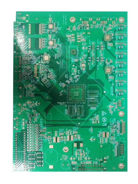
“Optimizing HDI PCB cost-performance balance: Key factors in design complexity, via-in-pad efficiency, and material selection for high-density applications while minimizing expenses.”
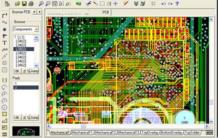
Introduction In the rapidly advancing world of electronics design, Circuit Board Computer-Aided Design (CAD) software has become an indispensable tool for engineers, hobbyists, and manufacturers alike. These sophisticated programs have revolutionized how printed circuit boards (PCBs) are conceptualized, designed, and prepared for production. From simple single-layer boards to complex multi-layer designs with high-density interconnects, PCB…
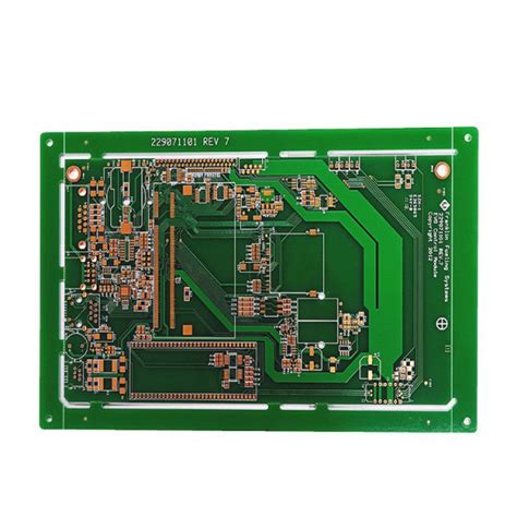
“HDI multilayer PCBs revolutionize electronics with ultra-compact designs, leveraging advanced layering and microvia technology to achieve superior circuit density for next-gen devices.” (239 characters)

“Master essential PCB design guidelines for reliable electronics manufacturing. Discover proven techniques adhering to industry best practices and mil-spec standards.”
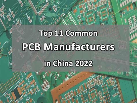
“Explore 2023’s top global PCB manufacturers shaping electronics innovation. Discover leaders in rigid, flex, and HDI boards driving cutting-edge solutions across industries worldwide.”
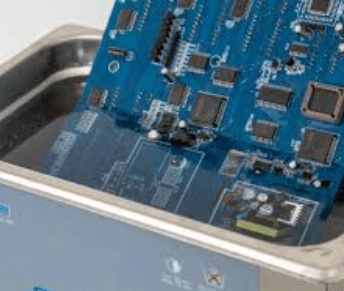
1. Introduction to Ultrasonic PCB Cleaners Printed Circuit Boards (PCBs) are essential components in modern electronics, found in everything from consumer gadgets to industrial machinery. Ensuring their cleanliness is crucial for performance, reliability, and longevity. Traditional cleaning methods, such as manual brushing or chemical baths, often fall short in removing microscopic contaminants. Ultrasonic PCB cleaners…
“Get your PCB made effortlessly with 24-hour turnaround & budget-friendly rates. Streamline prototyping using precision manufacturing and expert support. Start now!”
“Master Gerber-to-PCB conversion for error-free circuit board manufacturing. Discover efficient file processing techniques, layer alignment strategies, and industry-approved standards to accelerate prototype development.”
“Master Gerber file creation for efficient PCB prototyping. Learn industry standards & best practices to translate designs into manufacturable boards, accelerating hardware development.”
“Master Gerber file creation for reliable PCB manufacturing. Learn formatting standards, layer configuration, and error-free design practices to streamline production workflows.”

“Master Gerber fabrication best practices for PCB success: optimize RS-274X/X2, ODB++, IPC-2581 file formats. Collaborate with fabricators to verify requirements & ensure seamless manufacturing outcomes.”
“Master Gerber file fundamentals for seamless PCB production. Learn to translate designs into precise manufacturing specs using Gerber, ODB++, and IPC-2581 formats. Ensure board accuracy and manufacturability.”
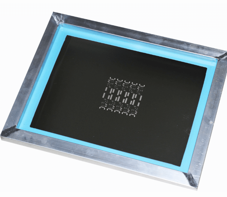
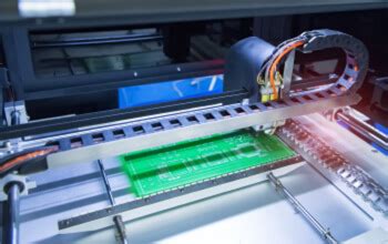
Introduction Surface Mount Technology (SMT) has revolutionized the electronics manufacturing industry by enabling the production of smaller, faster, and more efficient printed circuit boards (PCBs). A critical component in the SMT assembly process is the surface mount stencil, also known as an SMT stencil or solder paste stencil. This thin sheet, typically made of stainless…
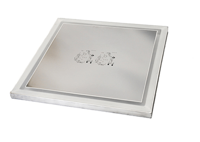
Introduction to PCB Stencils Printed Circuit Board (PCB) stencils, also known as solder paste stencils, are fundamental tools in modern electronics manufacturing. These precision tools serve as the bridge between PCB design and physical assembly, enabling the accurate deposition of solder paste onto circuit boards prior to component placement. A PCB stencil is essentially a…
We use cookies to improve your experience on our site. By using our site, you consent to cookies.
Manage your cookie preferences below:
Essential cookies enable basic functions and are necessary for the proper function of the website.
Statistics cookies collect information anonymously. This information helps us understand how visitors use our website.
Google Analytics is a powerful tool that tracks and analyzes website traffic for informed marketing decisions.
Service URL: policies.google.com (opens in a new window)
SourceBuster is used by WooCommerce for order attribution based on user source.
You can find more information in our privacy policy and privacy policy.