
The concepts and differences between FPGA and CPLD
Basic concepts of FPGA and CPLD
1.CPLD
CPLD is mainly composed of a programmable interconnect matrix unit around a programmable logic macro cell (LMC). The LMC logic structure is relatively complex and has a complex I/O unit interconnection structure. Users can generate specific circuit structures according to their needs to complete certain functions. Since the CPLD uses metal wires of fixed length to interconnect the logic blocks, the designed logic circuit has time predictability, avoiding the disadvantage of incomplete timing prediction of the segmented interconnection structure. By the 1990s, CPLD developed more rapidly, not only with electrical erasure characteristics, but also with advanced features such as edge scanning and online programmability. The more commonly used ones are Xilinx’s EPLD and Altera’s CPLD.
2.FPGA
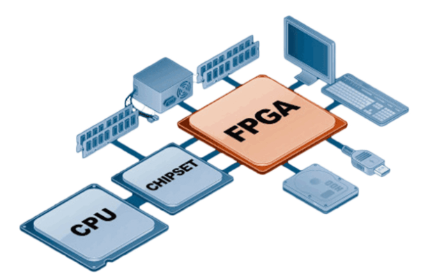
FPGA usually contains three types of programmable resources: programmable logic function blocks, programmable I/O blocks, and programmable interconnects. Programmable logic function blocks are the basic units for realizing user functions. They are usually arranged in an array and spread throughout the chip. Programmable I/O blocks complete the interface between the logic on the chip and the external package pins, and are often arranged around the array around the chip. Programmable internal interconnection includes wire segments of various lengths and some programmable connection switches, which connect various programmable logic blocks or I/O blocks. FPGAs have great differences in the scale of programmable logic blocks, the structure of internal interconnection lines, and the programmable elements used. The more commonly used ones are FPGAs from Altera, Xinlinx, and Actel.
FPGAs are generally used for logic simulation. When designing a circuit, circuit design engineers must first determine the circuit, and then perform software simulation and optimization to confirm the function and performance of the designed circuit. However, as the scale of the circuit continues to increase and the operating frequency continues to increase, many distributed parameter effects will be introduced into the circuit, and these effects are difficult to reflect using software simulation methods, so it is necessary to do hardware simulation. FPGA can implement hardware simulation to make a model machine. After the circuit simulated by software is processed and downloaded to FPGA, a model machine can be easily obtained. From this model machine, the designer can intuitively test its logic function and performance indicators.
Differences between FPGA and CPLD
Although FPGA and CPLD are both programmable ASIC devices with many common features, they have their own characteristics due to the differences in the structure of CPLD and FPGA:
①CPLD is more suitable for completing various algorithms and combinational logic, while FPGA is more suitable for completing sequential logic.
In other words, FPGA is more suitable for structures with rich triggers, while CPLD is more suitable for structures with limited triggers and rich product terms.
②The continuous wiring structure of CPLD determines that its timing delay is uniform and predictable, while the segmented wiring structure of FPGA determines the unpredictability of its delay.
③FPGA has greater flexibility in programming than CPLD.
CPLD is programmed by modifying the logic function with fixed internal circuits, and FPGA is mainly programmed by changing the wiring of internal connections; FPGA can be programmed under logic gates, while CPLD is programmed under logic blocks.
④FPGA has a higher integration than CPLD, and has a more complex wiring structure and logic implementation.
⑤CPLD is more convenient to use than FPGA.
CPLD programming uses E2PROM or FASTFLASH technology, does not require external memory chips, and is simple to use. However, the programming information of FPGA needs to be stored in external memory, and the method of use is complicated.
⑥CPLD is faster than FPGA and has greater time predictability.
This is because FPGA is gate-level programming, and distributed interconnection is used between CLBs, while CPLD is logic block-level programming, and the interconnection between its logic blocks is lumped.
⑦In terms of programming method, CPLD is mainly based on E2PROM or FLASH memory programming, and the number of programming times can reach 10,000 times.
The advantage is that the programming information is not lost when the system is powered off. CPLD can be divided into two categories: programming on the programmer and programming in the system. Most FPGAs are based on SRAM programming, and the programming information is lost when the system is powered off. Each time the power is turned on, the programming data needs to be rewritten to the SRAM from the outside of the device. Its advantage is that it can be programmed any number of times and can be programmed quickly during work, thus achieving dynamic configuration at the board level and system level.
⑧CPLD has good confidentiality, while FPGA has poor confidentiality.
⑨Generally speaking, the power consumption of CPLD is greater than that of FPGA, and the higher the integration, the more obvious it is.
With the increase in the density of complex programmable logic devices (CPLDs), digital device designers are flexible and easy when carrying out large-scale designs, and products can quickly enter the market. Many designers have already felt the advantages of CPLDs, such as predictable timing and high speed. However, in the past, due to the limitations of CPLD density, they had to turn to FPGAs and ASICs. Now, designers can experience the benefits of CPLDs with a density of up to hundreds of thousands of gates.
More embedded, Internet of Things, and smart hardware learning exchanges
