
Skip to content
Andwin Circuits
  • Home
  • ProductsExpand
    • HDI multilayer PCB
    • Rigid Flex PCB
    • Flex pcb
    • Special PCBExpand
      • High Frequency PCBExpand
        • Rogers RO4350B PCB
        • Rogers RO4003 pcb
        • Rogers RO3003 PCB
        • Rogers 5880 PCB
        • DICLAD 527 PCB
        • Taconic TLX series
        • Taconic TLX-8 RF PCB
        • Taconic TLX-9 RF PCB
      • High speed pcbExpand
        • Megtron 6 High Speed PCB
        • TU-872 SLK Sp High Speed
      • High TG PCBExpand
        • SHENGYI SH260 PCB
        • ISOLA 370HR PCB
        • ISOLA IS410 PCB
        • ISOLA IS420 PCB
      • Heavy copper PCB
      • Copper coin pcb
      • Copper inlay PCB
    • Metal Core PCBExpand
      • Copper core pcb
      • Aluminum PCB
      • 2 Layers Aluminum PCB
      • Direct thermal MCPCB
      • 2 Layers Direct Thermal
    • Ceramic PCBExpand
      • DPC ceramic PCB
      • DBC ceramic PCB
      • Thick film Ceramic PCB
      • Al2O3 Alumina PCB
      • AIN ALN ceramic PCB
      • IGBT Ceramic PCB
  • ServiceExpand
    • PCB Assembly
    • Quick turn PCB assembly
    • PCBA conformal coating
  • IndustryExpand
    • Telecommunication
    • IoT and Wireless
    • Industrial Control
    • Thermal management
    • Power and Energy
    • IC test board
    • Automative
    • Medical
  • CapabilityExpand
    • Rigid PCB
    • Rigid flex PCB
    • Metal core PCB
    • PCB Assembly
  • TechnologyExpand
    • Blogs
    • Via in pad
    • PCB E-test
    • PCB stack up
    • MCPCB panelization
    • Controlled impedance PCB
  • AboutExpand
    • About us
    • Certification
    • Factory Tour
  • Contact
Andwin Circuits
Home / The Failure Mechanisms Behind Poor Solder Wetting Phenomena

The Failure Mechanisms Behind Poor Solder Wetting Phenomena

ByGrace May 12, 2025May 10, 2025

Abstract

Poor solder wetting, commonly referred to as “non-wetting” or “dewetting,” is a critical defect in soldering processes that significantly impacts the reliability of electronic assemblies. This paper explores the underlying failure mechanisms contributing to poor solder wetting, including surface contamination, oxidation, intermetallic compound (IMC) formation, flux inefficiency, and thermal profile mismanagement. By analyzing these factors, we propose mitigation strategies to enhance solder joint integrity in surface mount technology (SMT) and through-hole soldering applications.

Keywords: solder wetting, non-wetting, intermetallic compounds, flux activity, thermal management, surface contamination

1. Introduction

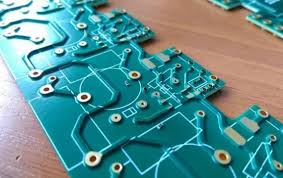
Solder wetting is a fundamental process in electronics manufacturing, where molten solder forms a metallurgical bond with component leads and printed circuit board (PCB) pads. Poor wetting leads to weak solder joints, increasing the risk of electrical failures and mechanical fractures. Understanding the root causes of this defect is essential for improving soldering quality in high-reliability applications.

2. Fundamentals of Solder Wetting

Wetting occurs when molten solder spreads over a metal surface due to favorable surface energy interactions. The process depends on:

  • Surface cleanliness (absence of oxides and contaminants)
  • Thermal conditions (adequate temperature for flux activation and solder flow)
  • Metallurgical compatibility (formation of stable IMCs)

When wetting fails, the solder either retracts (dewetting) or fails to spread (non-wetting), leaving exposed base metal.
Contact us for PCB quote now |

3. Key Failure Mechanisms

3.1 Surface Contamination

Contaminants such as oils, dust, or residual chemicals disrupt solder adhesion. Common sources include:

  • Fingerprints (organic residues)
  • Silicone contamination from mold release agents
  • Inadequate PCB cleaning post-fabrication

Mitigation:

  • Use plasma cleaning or alcohol-based degreasers.
  • Implement strict handling protocols (gloves, cleanroom practices).

3.2 Oxidation of Surfaces

Metallic surfaces (Cu, Ni, Sn) oxidize when exposed to air, forming barriers (e.g., Cu₂O, SnO₂) that repel molten solder.

Mitigation:

  • Store PCBs and components in nitrogen cabinets.
  • Use no-clean fluxes with strong reducing agents.

3.3 Intermetallic Compound (IMC) Issues

Excessive IMC growth (e.g., Cu₆Sn₅, Cu₃Sn) due to prolonged high temperatures can weaken joints and hinder wetting.

Mitigation:

  • Optimize reflow profiles to minimize dwell time above liquidus.
  • Use solder alloys with slower IMC growth rates (e.g., SAC305 vs. SnPb).

3.4 Flux Inefficiency

Flux removes oxides and promotes wetting, but insufficient activity or expired flux leads to failures.

Mitigation:

  • Select flux formulations matching the soldering method (e.g., RA flux for wave soldering).
  • Monitor flux storage conditions (humidity, temperature).

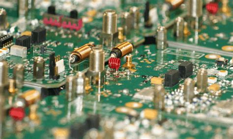
3.5 Thermal Profile Mismanagement

Incorrect reflow or wave soldering temperatures cause:

  • Cold joints (insufficient heat)
  • Solder balling (excessive heat)

Mitigation:

  • Use thermocouples to validate oven profiles.
  • Adjust preheat zones to ensure gradual temperature rise.
Contact us for PCB quote now |

4. Case Studies

4.1 Dewetting on ENIG (Electroless Nickel Immersion Gold) Pads

Root Cause: Nickel surface passivation due to excessive phosphorus content in the ENIG layer.
Solution: Optimize Ni-P plating bath chemistry to maintain <7% phosphorus.

4.2 Non-Wetting on OSP (Organic Solderability Preservative) Coated PCBs

Root Cause: OSP degradation from prolonged storage.
Solution: Reduce shelf life or switch to alternative finishes (e.g., Immersion Ag).

5. Advanced Analysis Techniques

  • SEM/EDS: Identifies surface contaminants and IMC composition.
  • Wetting Balance Tests: Quantifies wetting force and time.
  • X-ray Inspection: Detects voids and subsurface defects.

6. Conclusion

Poor solder wetting stems from multifaceted interactions between material properties, process parameters, and environmental conditions. By addressing contamination, oxidation, IMC formation, flux performance, and thermal management, manufacturers can significantly reduce soldering defects. Future work should explore nano-coated surfaces and low-temperature solder alloys to further enhance wetting reliability.

Contact us for PCB quote now |
Post Tags: #aluminum clad pcb#aluminum core pcb#aluminum pcb#pcb poor solder wetting phenomena

Post navigation

Previous Previous
Why Are PCBs Green? The Science and History Behind the Color of Circuit Boards
NextContinue
Key Considerations for PCB Design: What You Need to Know Before Drawing a PCB

Search

Search

Products

  • HDI Multilayer PCB
  • Rigid Flex PCB
  • Flex pcb
  • High Frequency PCB
  • High speed pcb
  • Heavy copper PCB
  • Metal Core PCB
  • Ceramic PCB

Address

Andwin Circuits Co.,Limited
Email: sales@andwinpcb.com
Tel: +86 755 2832 9394
Fax:+86 755 2992  6717
ADD:1-2F-1217,HouDeQun Industrial park,
NanTing RD NO.56,ShaJing,BaoAn,Shenzhen 518104,GuangDong,China

Products

  • HDI Multilayer PCB
  • Rigid Flex PCB
  • Flex pcb
  • High Frequency PCB
  • High speed pcb
  • Heavy copper PCB
  • Metal Core PCB
  • Ceramic PCB

Technology

  • Blogs
  • Via in pad
  • PCB E-test
  • PCB stack up
  • Metal core PCB panelization
  • Controlled impedance PCB

CERTIFICATION

Certification >>


Copyright© 2003 - 2026 Andwin | All Rights Reserved | Powered by Andwin

Scroll to top
  • Home
  • Products
    • HDI multilayer PCB
    • Rigid Flex PCB
    • Flex pcb
    • Special PCB
      • High Frequency PCB
        • Rogers RO4350B PCB
        • Rogers RO4003 pcb
        • Rogers RO3003 PCB
        • Rogers 5880 PCB
        • DICLAD 527 PCB
        • Taconic TLX series
        • Taconic TLX-8 RF PCB
        • Taconic TLX-9 RF PCB
      • High speed pcb
        • Megtron 6 High Speed PCB
        • TU-872 SLK Sp High Speed
      • High TG PCB
        • SHENGYI SH260 PCB
        • ISOLA 370HR PCB
        • ISOLA IS410 PCB
        • ISOLA IS420 PCB
      • Heavy copper PCB
      • Copper coin pcb
      • Copper inlay PCB
    • Metal Core PCB
      • Copper core pcb
      • Aluminum PCB
      • 2 Layers Aluminum PCB
      • Direct thermal MCPCB
      • 2 Layers Direct Thermal
    • Ceramic PCB
      • DPC ceramic PCB
      • DBC ceramic PCB
      • Thick film Ceramic PCB
      • Al2O3 Alumina PCB
      • AIN ALN ceramic PCB
      • IGBT Ceramic PCB
  • Service
    • PCB Assembly
    • Quick turn PCB assembly
    • PCBA conformal coating
  • Industry
    • Telecommunication
    • IoT and Wireless
    • Industrial Control
    • Thermal management
    • Power and Energy
    • IC test board
    • Automative
    • Medical
  • Capability
    • Rigid PCB
    • Rigid flex PCB
    • Metal core PCB
    • PCB Assembly
  • Technology
    • Blogs
    • Via in pad
    • PCB E-test
    • PCB stack up
    • MCPCB panelization
    • Controlled impedance PCB
  • About
    • About us
    • Certification
    • Factory Tour
  • Contact
Search