
The Purpose of PCB Exposure in the Printed Circuit Board Manufacturing Process
Introduction
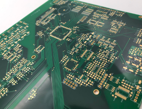
Printed Circuit Board (PCB) manufacturing is a complex, multi-step process that transforms a design into a functional board. One of the most critical stages in this process is exposure, which occurs during the photolithography stage. Exposure is essential for accurately transferring the circuit pattern from a photomask (or film) onto the PCB’s photosensitive layer. This step ensures precision in defining conductive traces, pads, and other critical features.
This article explores the purpose of PCB exposure, its role in the manufacturing process, the different exposure methods, and the factors affecting exposure quality. By understanding this step, engineers and manufacturers can optimize their processes for better yield and performance.
1. The Role of Exposure in PCB Manufacturing
1.1 Defining the Circuit Pattern
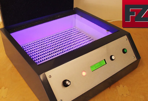
The primary purpose of exposure is to transfer the desired circuit pattern onto the PCB’s photosensitive resist layer. Before exposure, the board is coated with a photoresist (either liquid or dry film). The photoresist is then exposed to ultraviolet (UV) light through a photomask containing the circuit design.
- Positive Photoresist: Areas exposed to UV light become soluble and are removed during development.
- Negative Photoresist: Unexposed areas dissolve, leaving the exposed regions to form the circuit pattern.
This step ensures that only the intended copper traces remain after etching, preventing short circuits or open traces.
1.2 Enabling High Precision and Miniaturization
Modern PCBs require extremely fine traces (sometimes as small as 10–20 microns). Exposure allows for high-resolution pattern transfer, enabling:
- High-Density Interconnect (HDI) PCBs – Supports microvias and ultra-fine pitch components.
- Multilayer Boards – Ensures alignment accuracy between layers.
- Controlled Impedance Traces – Critical for high-frequency and RF applications.
Without precise exposure, advanced PCB designs would be impossible to manufacture reliably.
2. The PCB Exposure Process
2.1 Preparation Before Exposure
Before exposure, the PCB undergoes several preparatory steps:
- Cleaning – The copper-clad laminate is cleaned to remove contaminants.
- Photoresist Application – A light-sensitive resist is applied (via spray coating, roller coating, or dry film lamination).
- Pre-Baking – The resist is dried to remove solvents and improve adhesion.
2.2 Exposure Methods
There are two primary exposure techniques in PCB manufacturing:
A. Contact Exposure (Direct Exposure)
- The photomask is placed in direct contact with the PCB.
- Advantages: Simple, cost-effective, suitable for low-to-medium complexity designs.
- Disadvantages: Risk of mask wear, dust contamination, and reduced resolution due to light diffraction.
B. Projection Exposure (LDI – Laser Direct Imaging)
- Uses lasers to project the circuit pattern without a physical mask.
- Advantages:
- Higher precision (supports < 10µm features).
- No mask wear or alignment issues.
- Ideal for flexible and high-mix production.
- Disadvantages: Higher equipment cost.
2.3 Post-Exposure Steps
After exposure, the PCB undergoes:
- Development – The soluble resist is washed away, revealing the copper pattern.
- Etching – Unwanted copper is removed, leaving only the desired traces.
- Stripping – The remaining resist is removed, finalizing the conductive pattern.
3. Factors Affecting Exposure Quality
Several variables influence the success of the exposure process:
3.1 Light Source and Wavelength
- UV Light (365–405 nm) is commonly used due to its effectiveness with photoresists.
- Laser (355 nm or 405 nm) in LDI systems provides sharper edges for fine features.
3.2 Exposure Time and Intensity
- Overexposure can cause line widening, leading to short circuits.
- Underexposure may leave residual resist, causing etching defects.
3.3 Photomask Quality
- Dust, scratches, or misalignment can distort the pattern.
- High-resolution masks are crucial for fine-line PCBs.
3.4 Resist Type and Thickness
- Dry Film Resist: Better for thick traces but may have lower resolution.
- Liquid Resist: Allows finer features but requires precise coating.
3.5 Environmental Conditions
- Humidity and temperature can affect resist adhesion and exposure consistency.
4. Common Defects and Troubleshooting
4.1 Underexposure
- Symptoms: Incomplete resist development, poor etching.
- Solutions: Increase exposure time or UV intensity.
4.2 Overexposure
- Symptoms: Blurred traces, loss of fine details.
- Solutions: Reduce exposure duration or optimize mask alignment.
4.3 Misalignment
- Symptoms: Layer mismatches in multilayer PCBs.
- Solutions: Use automated optical alignment systems (AOI).
4.4 Dust and Contamination
- Symptoms: Random defects or pinholes.
- Solutions: Cleanroom conditions and regular mask maintenance.
5. Future Trends in PCB Exposure
5.1 Advanced LDI Systems
- Faster, higher-resolution laser imaging for next-gen PCBs.
5.2 AI-Based Process Optimization
- Machine learning for real-time exposure adjustments.
5.3 Eco-Friendly Photoresists
- Water-soluble and low-toxicity resists for sustainable manufacturing.
Conclusion
Exposure is a fundamental step in PCB manufacturing, ensuring accurate pattern transfer from design to board. It enables high-density interconnects, multilayer alignment, and fine-line circuitry. The choice between contact exposure and LDI depends on cost, precision, and production volume. By optimizing exposure parameters—such as light source, time, and resist type—manufacturers can minimize defects and improve yield.
As PCB technology advances toward finer pitches and flexible electronics, innovations in exposure techniques (such as LDI and AI-driven adjustments) will play a crucial role in meeting future demands. Understanding the exposure process is essential for engineers and manufacturers aiming to produce reliable, high-performance PCBs.
References (if needed, can be added per request)
This article provides a comprehensive overview of PCB exposure, its purpose, methods, challenges, and future trends while maintaining technical depth and readability. Let me know if you’d like any modifications or additional details!