
Skip to content
Andwin Circuits
  • Home
  • ProductsExpand
    • HDI multilayer PCB
    • Rigid Flex PCB
    • Flex pcb
    • Special PCBExpand
      • High Frequency PCBExpand
        • Rogers RO4350B PCB
        • Rogers RO4003 pcb
        • Rogers RO3003 PCB
        • Rogers 5880 PCB
        • DICLAD 527 PCB
        • Taconic TLX series
        • Taconic TLX-8 RF PCB
        • Taconic TLX-9 RF PCB
      • High speed pcbExpand
        • Megtron 6 High Speed PCB
        • TU-872 SLK Sp High Speed
      • High TG PCBExpand
        • SHENGYI SH260 PCB
        • ISOLA 370HR PCB
        • ISOLA IS410 PCB
        • ISOLA IS420 PCB
      • Heavy copper PCB
      • Copper coin pcb
      • Copper inlay PCB
    • Metal Core PCBExpand
      • Copper core pcb
      • Aluminum PCB
      • 2 Layers Aluminum PCB
      • Direct thermal MCPCB
      • 2 Layers Direct Thermal
    • Ceramic PCBExpand
      • DPC ceramic PCB
      • DBC ceramic PCB
      • Thick film Ceramic PCB
      • Al2O3 Alumina PCB
      • AIN ALN ceramic PCB
      • IGBT Ceramic PCB
  • ServiceExpand
    • PCB Assembly
    • Quick turn PCB assembly
    • PCBA conformal coating
  • IndustryExpand
    • Telecommunication
    • IoT and Wireless
    • Industrial Control
    • Thermal management
    • Power and Energy
    • IC test board
    • Automative
    • Medical
  • CapabilityExpand
    • Rigid PCB
    • Rigid flex PCB
    • Metal core PCB
    • PCB Assembly
  • TechnologyExpand
    • Blogs
    • Via in pad
    • PCB E-test
    • PCB stack up
    • MCPCB panelization
    • Controlled impedance PCB
  • AboutExpand
    • About us
    • Certification
    • Factory Tour
  • Contact
Andwin Circuits
Home / Blogs / Thermal pad pcb layout

Thermal pad pcb layout

ByGrace June 28, 2023June 15, 2024


There should be sufficient clearance around the thermal pad to avoid short circuits and ensure proper soldering.

4. Solder mask:

The solder mask should be removed from the thermal pad to allow for proper soldering.

5. Via placement:

Vias can be placed around the thermal pad to improve heat dissipation and reduce thermal resistance.

6. Thermal relief:

Thermal relief can be added to the thermal pad to make it easier to solder and reduce the risk of solder bridges.

Overall, the thermal pad on a PCB layout should be carefully designed to ensure proper heat dissipation and reliable operation of the component.
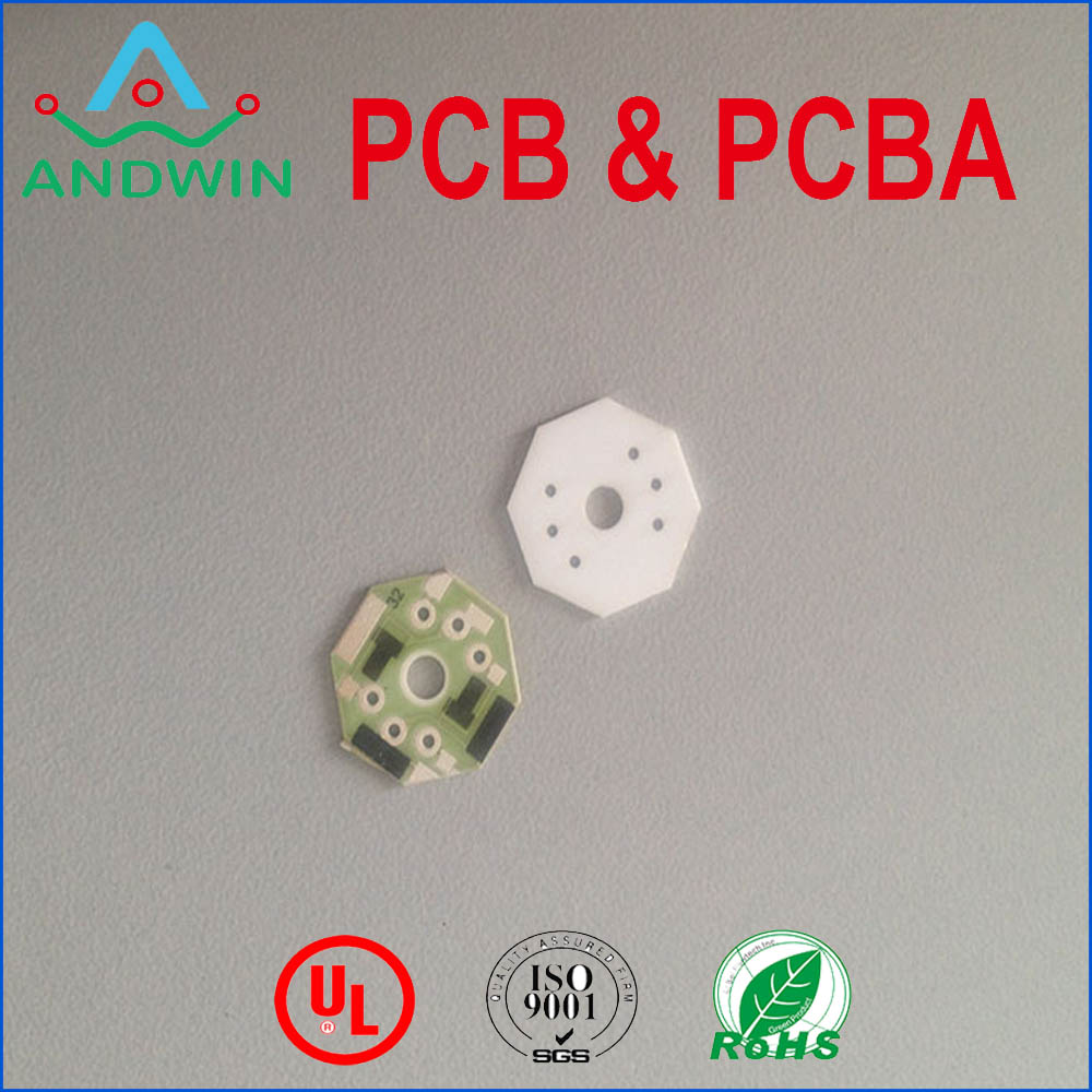
thermal pad pcb layout structure

A thermal pad on a PCB layout is typically a large copper area that is connected to a ground plane or a power plane.
The thermal pad is designed to provide a low thermal resistance path for heat dissipation from the component to the PCB.

The thermal pad is usually located directly under the component that generates heat, such as a power transistor or a voltage regulator.

The thermal pad is connected to the ground plane or power plane through a series of vias that are located around the perimeter of the pad.
The vias provide a low resistance path for heat to flow from the component to the ground plane or power plane.

The number and size of the vias depend on the amount of heat that needs to be dissipated and the size of the thermal pad.

The thermal pad should be designed to be as large as possible to provide the maximum surface area for heat dissipation.
The pad should also be located as close as possible to the component that generates heat to minimize the thermal resistance between the component and the pad.

In addition to the thermal pad, the PCB layout should also include a heat sink or a heat spreader to further enhance the heat dissipation.
The heat sink or heat spreader can be attached to the thermal pad using a thermal interface material (TIM) such as thermal paste or a thermal pad.

The TIM helps to fill any gaps between the heat sink or heat spreader and the thermal pad,
which improves the thermal conductivity between the two surfaces.

GET IN TOUCH!

Post navigation

Previous Previous
Ceramic PCB list – quality Ceramic PCB privided ceramic pcb process
NextContinue
Application of Ceramic PCB-Ceramic PCB Market

Search

Search

Products

  • HDI Multilayer PCB
  • Rigid Flex PCB
  • Flex pcb
  • High Frequency PCB
  • High speed pcb
  • Heavy copper PCB
  • Metal Core PCB
  • Ceramic PCB

Address

Andwin Circuits Co.,Limited
Email: sales@andwinpcb.com
Tel: +86 755 2832 9394
Fax:+86 755 2992  6717
ADD:1-2F-1217,HouDeQun Industrial park,
NanTing RD NO.56,ShaJing,BaoAn,Shenzhen 518104,GuangDong,China

Products

  • HDI Multilayer PCB
  • Rigid Flex PCB
  • Flex pcb
  • High Frequency PCB
  • High speed pcb
  • Heavy copper PCB
  • Metal Core PCB
  • Ceramic PCB

Technology

  • Blogs
  • Via in pad
  • PCB E-test
  • PCB stack up
  • Metal core PCB panelization
  • Controlled impedance PCB

CERTIFICATION

Certification >>


Copyright© 2003 - 2026 Andwin | All Rights Reserved | Powered by Andwin

Scroll to top
  • Home
  • Products
    • HDI multilayer PCB
    • Rigid Flex PCB
    • Flex pcb
    • Special PCB
      • High Frequency PCB
        • Rogers RO4350B PCB
        • Rogers RO4003 pcb
        • Rogers RO3003 PCB
        • Rogers 5880 PCB
        • DICLAD 527 PCB
        • Taconic TLX series
        • Taconic TLX-8 RF PCB
        • Taconic TLX-9 RF PCB
      • High speed pcb
        • Megtron 6 High Speed PCB
        • TU-872 SLK Sp High Speed
      • High TG PCB
        • SHENGYI SH260 PCB
        • ISOLA 370HR PCB
        • ISOLA IS410 PCB
        • ISOLA IS420 PCB
      • Heavy copper PCB
      • Copper coin pcb
      • Copper inlay PCB
    • Metal Core PCB
      • Copper core pcb
      • Aluminum PCB
      • 2 Layers Aluminum PCB
      • Direct thermal MCPCB
      • 2 Layers Direct Thermal
    • Ceramic PCB
      • DPC ceramic PCB
      • DBC ceramic PCB
      • Thick film Ceramic PCB
      • Al2O3 Alumina PCB
      • AIN ALN ceramic PCB
      • IGBT Ceramic PCB
  • Service
    • PCB Assembly
    • Quick turn PCB assembly
    • PCBA conformal coating
  • Industry
    • Telecommunication
    • IoT and Wireless
    • Industrial Control
    • Thermal management
    • Power and Energy
    • IC test board
    • Automative
    • Medical
  • Capability
    • Rigid PCB
    • Rigid flex PCB
    • Metal core PCB
    • PCB Assembly
  • Technology
    • Blogs
    • Via in pad
    • PCB E-test
    • PCB stack up
    • MCPCB panelization
    • Controlled impedance PCB
  • About
    • About us
    • Certification
    • Factory Tour
  • Contact
Search