
Thermal Relief in PCB Design: When and How to Use It
If you’ve struggled with cold solder joints during PCB assembly or pads that won’t reach soldering temperature, thermal relief design is the solution. This spoked copper pattern directly affects assembly yield, joint reliability, and rework success across through-hole and surface-mount manufacturing.
This guide explains what thermal relief is, when to use it versus direct connections, how spoke configurations affect solderability and electrical performance, and where high-current applications require exceptions. You will learn IPC design rules that balance assembly ease with thermal requirements.
What Is Thermal Relief in PCB Design?
Thermal relief is a spoked copper pattern connecting a pad or via to a copper plane (ground or power). Instead of solid connection, thermal relief uses 2 to 4 narrow spokes arranged radially. These maintain electrical connection while controlling heat flow during soldering.
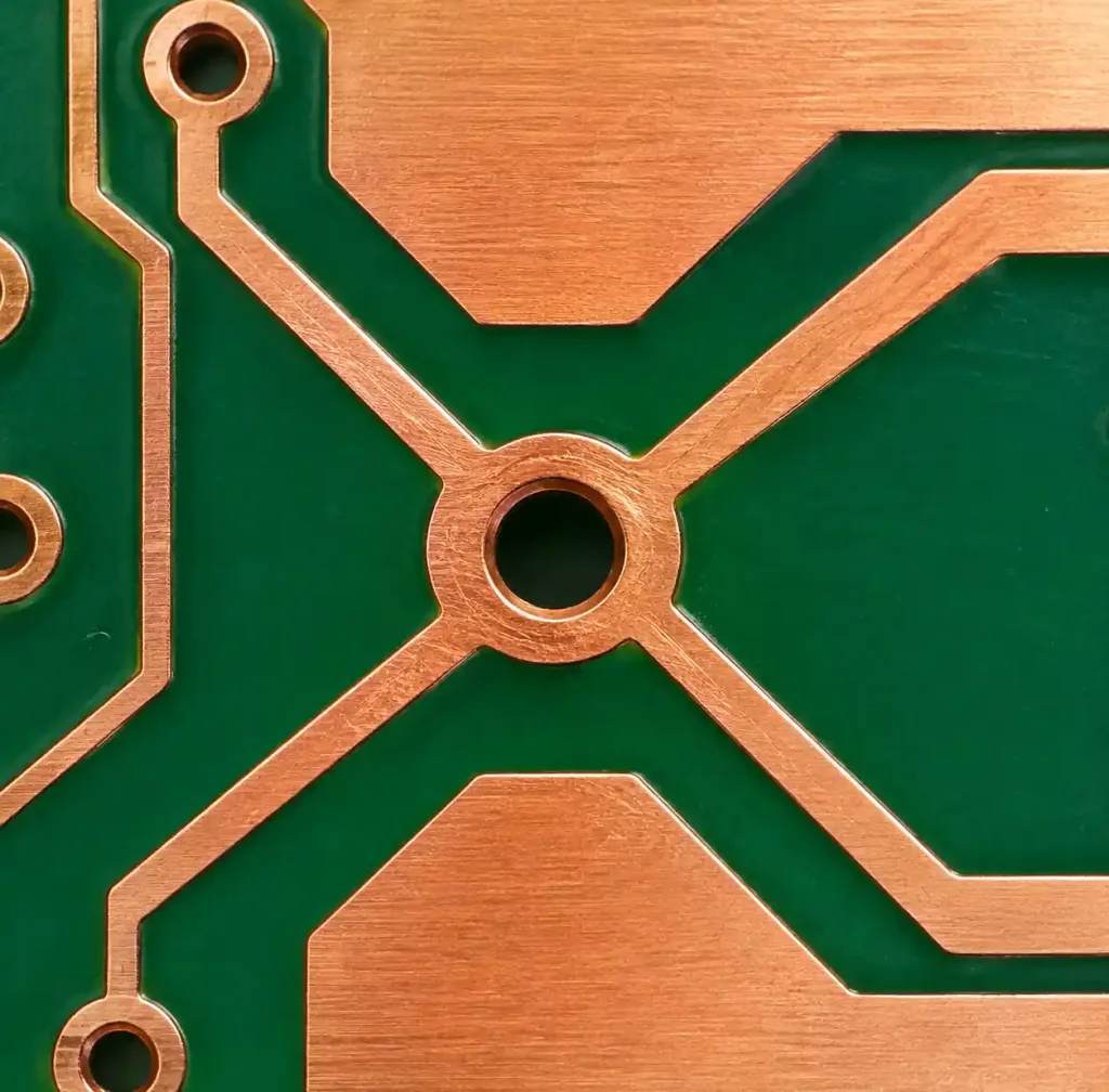
The primary purpose is solderability. Large copper planes act as heat sinks drawing thermal energy away during reflow or wave soldering. Without thermal relief, pads may not reach 217°C–245°C solder melting temperature, causing cold joints or insufficient wetting.
You recognize thermal relief by the cross or X-shaped spoke arrangement around pads connecting to planes. Standard practice specifies these for through-hole leads, vias to planes, and SMD pads on ground or power layers.
When to Use Thermal Relief
Standard Applications Requiring Thermal Relief
You should specify thermal relief for these pad types:
- Through-hole component pads: All PTH leads connecting to ground or power planes
- Vias to planes: Signal vias passing through or terminating at plane layers
- SMD pads on planes: Surface-mount pads on copper pour areas
- Test points: PCB test pads connected to reference planes
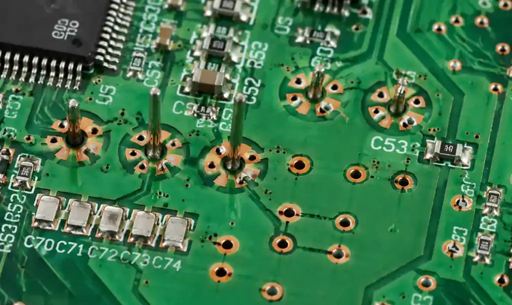
The principle is simple: any pad reaching soldering temperature while connected to large copper mass requires thermal relief. Without it, manual soldering becomes difficult and automated reflow may produce weak joints with incomplete intermetallic formation.
When Direct Connection Is Required
Direct connections (no thermal relief) are necessary for high-current and thermal management applications:
| Application Type | Connection Method | Current Threshold | Thermal Goal |
|---|---|---|---|
| High-current power traces | Direct | > 3A per pad | Minimize voltage drop |
| Power MOSFETs thermal pads | Direct | N/A | Maximum heat transfer |
| Heavy copper PCB (≥ 3oz) | Direct or reduced spoke | > 5A | Balance current and solderability |
| Thermal vias under ICs | Direct | N/A | Efficient heat spreading |
For these applications, accept the soldering difficulty. Techniques include board preheating to 100°C–150°C, higher-wattage soldering irons (80–150W), or longer reflow profiles with extended time above liquidus.
Spoke Configuration Design Rules
2-Spoke vs 4-Spoke Patterns
Spoke count affects both thermal isolation and mechanical strength:
4-Spoke Configuration (Standard):
- Spoke arrangement: 90° spacing (cross pattern)
- Typical spoke width: 0.20mm–0.30mm (8–12 mil)
- Typical spoke length: 0.25mm–0.50mm
- Applications: General PTH and SMD pads, standard layers
- Advantages: Better mechanical strength, redundancy
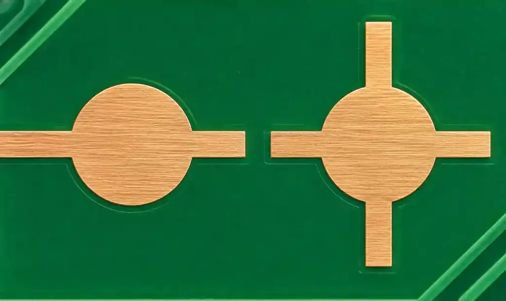
2-Spoke Configuration (High isolation):
- Spoke arrangement: 180° spacing (opposite sides)
- Typical spoke width: 0.15mm–0.25mm (6–10 mil)
- Applications: Small passives, low-current signals
- Advantages: Greater thermal resistance, faster pad heating
Spoke Width and Gap Specifications
IPC-2221 provides clearance guidelines, while spoke dimensions balance electrical, thermal, and manufacturing requirements:
| PCB Parameter | Minimum Value | Typical Value | Maximum Value |
|---|---|---|---|
| Spoke width | 0.10mm (4 mil) | 0.20mm–0.30mm (8–12 mil) | 0.50mm (20 mil) |
| Air gap (pad to plane) | 0.20mm (8 mil) | 0.30mm–0.40mm (12–16 mil) | 0.60mm (24 mil) |
| Spoke length | 0.15mm (6 mil) | 0.25mm–0.40mm (10–16 mil) | 0.80mm (32 mil) |
| Minimum annular ring | 0.10mm (4 mil) | 0.15mm (6 mil) | — |
Spoke width depends on current. For signal pads < 0.5A, use 0.15mm–0.25mm spokes. For power connections 1A–3A, increase to 0.30mm–0.50mm while maintaining thermal relief benefits.
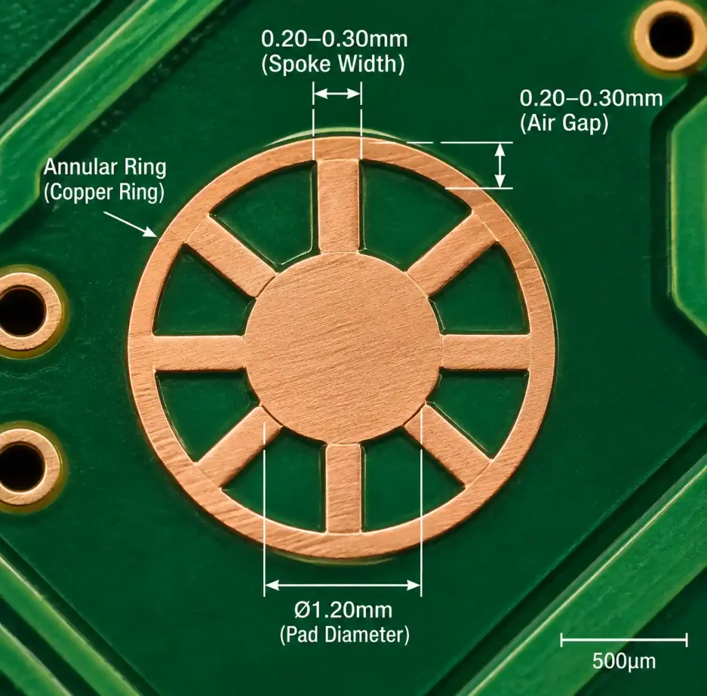
The air gap (clearance between pad and plane) must exceed minimum trace-to-plane clearance. Typical values are 0.30mm (12 mil) for standard PCBs and 0.40mm (16 mil) for IPC-6012 Class 3 high-reliability applications.
DFM Impact on Assembly and Reliability
Solderability and Reflow Effects
Thermal relief directly affects PCB assembly yield. During reflow, pads with proper thermal relief reach peak temperature 15°C–30°C higher than direct-connected pads, improving solder wetting and intermetallic formation.
Assembly considerations:
- Wave soldering: Thermal relief prevents solder bridging by limiting heat spread
- Selective soldering: Pads heat 40%–60% faster with 2-spoke relief versus direct
- Manual soldering: Operators require 30%–50% less dwell time on thermal-relief pads
- Rework: Significantly reduces board damage risk during component removal
Coordinate thermal relief specifications with your assembly house. Some request direct connections for power pads > 5A, accepting customized reflow profiles or wave solder preheat.
Mechanical Strength Considerations
Thermal relief improves solderability but slightly reduces mechanical pad strength. Spoke patterns create stress concentration under shock or vibration.
For high-reliability applications (automotive, aerospace, medical): use 4 spokes instead of 2 for better load distribution, widen spokes from 0.20mm to 0.30mm–0.40mm for power pads, add teardrops at spoke-pad junctions, and apply conformal coating after assembly.
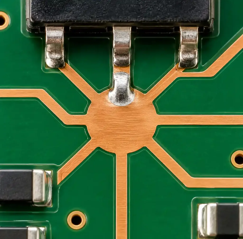
IPC-6012 Class 3 recommends 4-spoke thermal relief with minimum 0.25mm spoke width for all PTH pads connected to planes.
Automated vs Manual Thermal Relief Placement
CAD Tool Automatic Generation
Modern PCB design software (Altium, KiCad, Eagle, Allegro) automatically generates thermal relief based on design rules:
Typical settings: Connection style (spoke vs direct), spoke count (2 or 4), spoke width (0.20mm–0.30mm), air gap (0.30mm–0.40mm), rotation (45° X-pattern or 0° cross).
Define rules per net class:
- Signal nets: 4-spoke, 0.20mm width, 0.30mm gap
- Low-current power (< 1A): 4-spoke, 0.25mm width
- High-current power (> 3A): Direct connection
When to Override Automatic Rules
Manual placement control is necessary for:
- Mixed current on same net: Power plane with both signal and high-current connections
- Thermal management ICs: Power MOSFETs requiring direct thermal pad while other pins use relief
- Test point access: May require direct for current injection testing
- Repair considerations: Critical nodes where rework likelihood is high
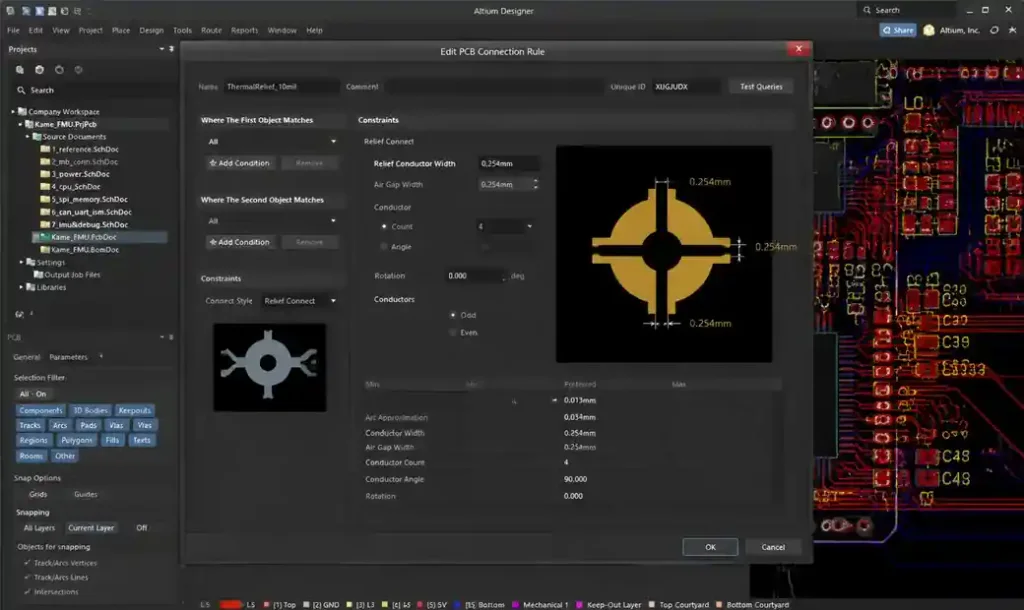
You can specify pad-specific overrides by setting individual pad connection properties rather than relying on net-class rules.
Special Cases and Exceptions
High-Frequency and RF Applications
In RF PCBs and high-speed digital designs above 1 GHz, thermal relief can affect impedance and signal integrity. Spokes create impedance discontinuities at via transitions between signal layers and reference planes.
For controlled impedance PCBs, consider:
- Keep vias close to ground: Minimize spoke length to reduce inductance (< 0.25mm)
- Use 4-spoke symmetric patterns: Maintains balanced impedance
- Simulate discontinuity impact: Use 3D EM simulation to verify S-parameters
- Via-in-pad applications: May require filled or plugged vias with modified relief
Heavy Copper PCB Design
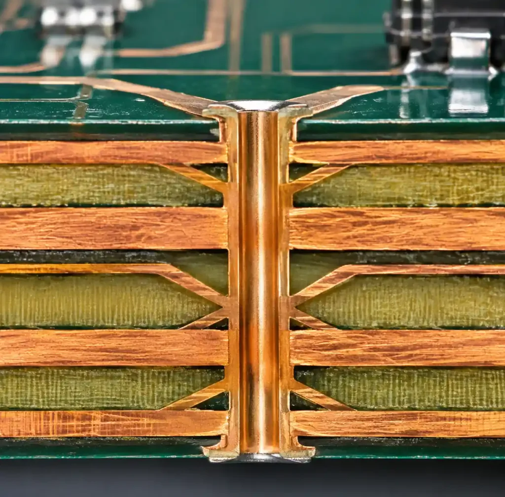
Heavy copper PCBs with copper weight ≥ 3oz (105μm) present unique challenges. Increased copper thickness creates larger heat sink mass, requiring wider spokes for current capacity.
Heavy copper thermal relief specifications:
| Copper Weight | Spoke Width | Spoke Count | Current Capacity |
|---|---|---|---|
| 2oz (70μm) | 0.25mm (10 mil) | 4 | Up to 2A |
| 3oz (105μm) | 0.40mm (16 mil) | 4 | Up to 4A |
| 4oz (140μm) | 0.50mm (20 mil) | 4 or direct | Up to 6A |
| 6oz+ (210μm+) | Direct connection | N/A | > 8A |
For power applications requiring both high current and acceptable solderability, use hybrid approaches: direct connection for power pads with preheating during assembly, and standard thermal relief for signal pads.
IPC Standards and Design Guidelines
IPC-2221 Generic PCB Design Standard
IPC-2221B Section 9.1.2: Thermal relief shall be used for all plated through-holes connected to large copper areas unless current requirements dictate otherwise. Minimum spoke width: 0.13mm (5 mil) for Class 1/2, 0.20mm (8 mil) for Class 3.
IPC-6012 Qualification Standard
IPC-6012 Class 3: Thermal relief connections must withstand thermal stress testing per IPC-TM-650 Method 2.6.8. Spoke dimensions must support rated current without exceeding 30°C temperature rise.
Frequently Asked Questions
When should I use 2-spoke versus 4-spoke thermal relief?
Use 4-spoke as standard for through-hole pads and vias for better mechanical strength and redundancy. Choose 2-spoke only for small passive components (0402, 0201) or situations requiring maximum thermal isolation for difficult soldering.
Can I use thermal relief on signal vias in high-speed designs?
Yes, thermal relief is necessary for signal vias to reference planes, but keep spoke length under 0.30mm to minimize impedance discontinuity. For critical nets above 5 GHz, simulate the via structure including thermal relief to verify signal integrity impact.
What happens if I forget thermal relief on some pads?
Pads without thermal relief on large copper planes will be difficult or impossible to solder properly. You’ll experience cold joints, insufficient wetting, or complete assembly failures. DFM review should catch this, but late changes may require board rework.
Do I need thermal relief on bottom-side SMD pads?
Yes, if those pads connect to ground or power copper pours. Large copper creates the same heat sink effect regardless of mounting side. Apply the same thermal relief rules to both top and bottom layers.
How does thermal relief affect power delivery network impedance?
Thermal relief spokes add small series resistance (0.5–2 mΩ per connection) and inductance (50–200 pH). For PDN design, this is usually negligible compared to via inductance and plane spreading inductance, but verify with PDN simulation for high-current applications > 10A.
Should I use thermal relief for PCB assembly test points?
Generally yes, as test points typically carry only measurement currents (< 100mA). Thermal relief makes test point soldering and rework easier. For test points used for in-circuit testing or power injection, consult your test strategy and current requirements.
Conclusion
Thermal relief is a fundamental PCB design technique balancing assembly solderability with electrical and thermal performance. Apply 4-spoke thermal relief as default for all through-hole and surface-mount pads attached to copper planes, using 0.20mm–0.30mm spoke widths and 0.30mm–0.40mm air gaps per IPC-2221 standards.
Reserve direct connections for high-current power paths above 3A, thermal management pads requiring maximum heat transfer, and heavy copper PCB applications where current capacity outweighs soldering convenience. Configure your CAD tool’s design rules to automatically generate appropriate thermal relief patterns.
Andwin Circuits manufactures PCBs with optimized thermal relief patterns from 4 to 50 layers, supporting standard and heavy copper configurations. Our DFM review verifies thermal relief placement meets IPC-6012 standards while accommodating your specific assembly and current requirements.
Contact us today for expert PCB manufacturing with proper thermal relief design and fast 7-day prototype delivery.