
Thick Copper PCB (6oz+): High Current Carrying Solutions for Power Modules
When you’re pushing 30A through a PCB trace, standard 1oz copper just doesn’t cut it. The trace gets hot, voltage drops across every inch, and you start looking at bus bars or heavy gauge wire. Thick copper PCBs—6oz and up—solve this by putting the conductor right in the board. Working with an experienced PCB manufacturer that understands heavy copper fabrication is critical—not every shop can handle the etching, plating, and lamination challenges that come with 6oz+ copper. Here’s what actually matters when designing for high current.
Why Thick Copper PCBs Matter
Standard boards use 1oz (35μm) or 2oz (70μm) copper. Fine for signals. Not fine for power. A 10mm trace in 1oz copper carrying 30A gets hot enough to worry about. Bump that to 6oz (210μm) and the same trace handles the current with acceptable temperature rise.
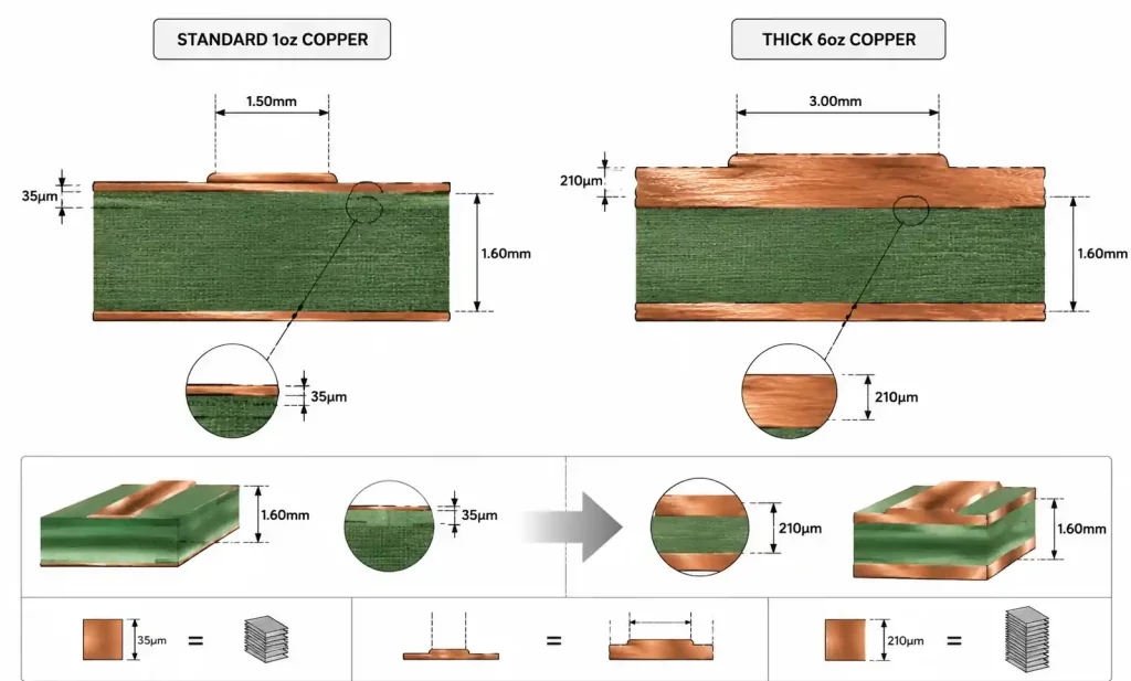
You need thick copper when: continuous current exceeds 15-20A per trace, you need to keep voltage drop under 50-100mV, operating temps are above 85°C, or you want to integrate power stages and control logic on the same board without external bus bars.
Typical applications: DC-DC converters above 500W, three-phase motor drives, EV battery management systems, welding equipment, solar inverters, and high-power LED drivers.
Current Capacity: Copper Weight vs Trace Width
IPC-2152 is the standard you should be using—not the old IPC-2221 nomographs. For thick copper, thermal mass and cross-section let you push significantly more current before hitting temperature rise limits.
| Copper Weight | Trace Width | Max Current (10°C rise) | Max Current (30°C rise) | Resistance (per inch) |
|---|---|---|---|---|
| 6oz (210μm) | 5mm | 22A | 35A | 0.25 mΩ |
| 6oz (210μm) | 10mm | 38A | 60A | 0.125 mΩ |
| 8oz (280μm) | 5mm | 26A | 42A | 0.19 mΩ |
| 8oz (280μm) | 10mm | 45A | 70A | 0.095 mΩ |
| 10oz (350μm) | 5mm | 30A | 48A | 0.15 mΩ |
| 10oz (350μm) | 10mm | 52A | 80A | 0.075 mΩ |
Internal layers, FR-4, 1oz base on outer, 25°C ambient. Outer layers with better cooling get 10-15% more. Enclosed or hot environments? Derate 20-30%.
Resistance matters more than you’d think. 0.25 mΩ per inch at 30A is 225mW per inch of copper. Run that for six inches and you’ve got over a watt of heat right there.
Design Rules for Heavy Copper
Thick copper changes the fabrication game. Etching takes longer, sidewalls taper, vias plate differently.
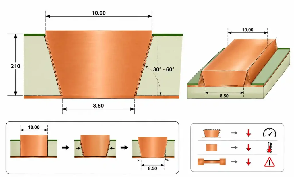
Trace and space: For 6oz, minimum trace is usually 8-10 mils, but spacing is the real constraint. 3oz gets you 8-10 mils. 6oz needs 12-15 mils. 8oz and above push 15-20 mils. The etch taper eats into your design rule—what’s 10mm at the top might be 8.5mm at the base. Always design to the minimum width.
Clearance: If you’re running 300V DC (PFC stages, anyone?), IPC-2221 wants 0.6mm (24 mils) for uncoated boards. That trumps manufacturing minimums every time.
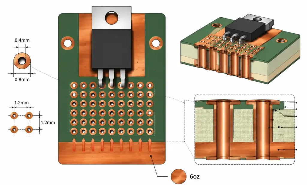
Vias: Standard 0.3mm drill with 0.6mm pad works for 1oz. For 6oz, step up to 0.4mm hole with 0.8mm pad. 8oz+ needs 0.5mm hole and 1.0mm pad. Via-in-pad adds 15-25% cost. Thermal vias under a TO-220 at 5W? Usually 12-16 vias. With 6oz planes, you can get away with 8-10 because the copper spreads heat better.
Manufacturing Realities
Not every fab can do heavy copper. The ones that can have longer lead times and higher costs.
Process differences: Etching 6oz takes longer, needs different chemistry, requires tighter process control. Lead times stretch from 7-10 days to 15-18 days. Lamination is trickier—thick copper creates topology that messes with resin flow. Manufacturers compensate with extra prepreg plies or low-flow materials, which affects your stackup. For designers working with high-density interconnects in power modules, HDI flex PCB structures with 3+N+3 buildup face similar lamination and registration challenges—many of the same DFM principles apply.
Cost: Figure 2-3× the price of standard copper. Material costs more, processing takes longer, yields are worse, tooling is specialized. Expedite fees for prototypes under 10 days can run 50-100% extra.
Stackup Design for Power Modules
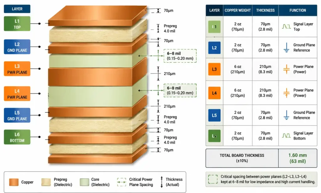
You’ve got high-current switching, gate drive, control logic, and maybe isolated supplies all on one board. Here’s a stackup that works.
| Layer | Function | Copper Weight | Notes |
|---|---|---|---|
| L1 (Top) | Signal + low-current power | 2oz | Components, gate drive |
| L2 (Plane) | GND | 2oz | Continuous ground |
| L3 (Plane) | High-current positive rail | 6oz | Main power distribution |
| L4 (Plane) | High-current return / negative | 6oz | Power return path |
| L5 (Plane) | Isolated GND or auxiliary | 2oz | Secondary ground domain |
| L6 (Bottom) | Signal + low-current power | 2oz | Control, feedback |
Keep the dielectric between L3 and L4 thin (6-8 mils) to minimize loop inductance. This matters for hard-switched topologies with high dV/dt and di/dt. Gate drive traces on L1? Keep 50Ω if your MOSFET rise times are under 20ns.
DFM Checklist for Heavy Copper
Common gotchas:
- Undercut: The sidewall taper means a 10mm trace might only be 8.5mm at the base. Add 10-15% width margin.
- Solder mask registration: Thick copper creates surface relief. Mask dams need at least 8 mils between high-voltage nodes.
- Plating uniformity: 0.3mm drill in a 2.4mm board is an 8:1 aspect ratio—right at the limit. Use 0.4mm+ drills.
- Bow and twist: Asymmetric copper distribution causes warp. Keep your stackup balanced.
Pre-flight check:
- [ ] Spacing meets manufacturer capability (12-15 mils for 6oz)
- [ ] Edge clearance >40 mils for 6oz planes
- [ ] Via pads sized for copper thickness (0.4mm min hole for 6oz)
- [ ] Power traces have 10-15% margin
- [ ] Solder mask dams ≥8 mils after registration tolerance
- [ ] Stackup is symmetric or near-symmetric
- [ ] Drill aspect ratios under 8:1
Alternatives: When Thick Copper Isn’t the Answer
Above 60-80A, bus bars or copper straps start making more sense than PCB traces. A 0.5mm copper bar is cheaper than 12oz PCB copper, easier to assemble, and gives you lower inductance—but assembly gets more complicated.
Heatsinking can sometimes let you drop copper weight. If you’ve got a big heat sink, 4oz might do the job instead of 8oz, saving 30-40% on board cost. Run thermal simulations early.
Parallel traces on multiple layers can replace a single thick layer. Two 10mm traces in 3oz copper (one per layer) carry similar current to one 10mm trace in 6oz, with more routing flexibility and potentially lower cost. Downside: more layers and via stitching to balance current.
Aluminum-core PCBs offer better thermal performance for concentrated heat sources. A 1.5mm aluminum core with 3oz copper often outperforms FR-4 with 6oz, at similar cost. But you’re limited to 1-2 layers.
FAQ
Can I mix copper weights on different layers?
Yes—standard practice. 6oz or 8oz on power layers, 1oz or 2oz on signals. The stackup needs to account for thickness differences in impedance calculations, and the fab needs to balance prepreg to handle the relief. Expect a 10-15% cost premium over uniform copper.
How do I calculate temperature rise for a trace?
Use IPC-2152 charts or an online calculator based on that standard. You need copper weight, trace width and length, current, ambient temp, and whether it’s internal or external. Internal layers get derated based on adjacent planes and board thermal resistance. Target 10°C rise for reliability-critical, 30°C for cost-optimized commercial.
What surface finish works for thick copper power pads?
ENIG is the default—flat surface, handles multiple reflow cycles, good shelf life. Immersion silver costs less but has shorter shelf life. HASL is uneven and can be problematic for press-fit connectors. For wire bonding, specify hard gold over nickel, 30-50 microinches.
How does thick copper affect impedance control?
Thick copper increases the distance between trace and reference plane, raising impedance. For 50Ω traces, you need to reduce trace width or increase dielectric thickness. Practical solution: route high-speed signals on outer layers with standard 1-2oz copper and keep thick copper on internal power planes.
Conclusion
Thick copper PCBs let you push 20-80A through the board without external bus bars. The catch: 2-3× the cost and longer lead times. Worth it when you need the density.
Design rules that save you from respins: Use IPC-2152 for current calcs, not the old charts. Add 10-15% margin on trace widths for etch taper. Keep power planes thin on dielectric for loop inductance. Balance your stackup or it’ll warp. Get a DFM review before you fab.
When it’s not the answer: Over 60-80A, bus bars are cheaper and easier. Big heatsinks might let you drop to 4oz. Parallel traces can sometimes do the job with less cost. Aluminum-core PCBs are worth a look if heat is your real problem.
Thick copper isn’t complicated—it’s just copper with tighter rules and higher costs. Get the layout right, work with a PCB manufacturer that knows what they’re doing, and your board will handle the current without burning up.