Skip to content
Andwin Circuits
  • Home
  • ProductsExpand
    • HDI multilayer PCB
    • Rigid Flex PCB
    • Flex pcb
    • Special PCBExpand
      • High Frequency PCBExpand
        • Rogers RO4350B PCB
        • Rogers RO4003 pcb
        • Rogers RO3003 PCB
        • Rogers 5880 PCB
        • DICLAD 527 PCB
        • Taconic TLX series
        • Taconic TLX-8 RF PCB
        • Taconic TLX-9 RF PCB
      • High speed pcbExpand
        • Megtron 6 High Speed PCB
        • TU-872 SLK Sp High Speed
      • High TG PCBExpand
        • SHENGYI SH260 PCB
        • ISOLA 370HR PCB
        • ISOLA IS410 PCB
        • ISOLA IS420 PCB
      • Heavy copper PCB
      • Copper coin pcb
      • Copper inlay PCB
    • Metal Core PCBExpand
      • Copper core pcb
      • Aluminum PCB
      • 2 Layers Aluminum PCB
      • Direct thermal MCPCB
      • 2 Layers Direct Thermal
    • Ceramic PCBExpand
      • DPC ceramic PCB
      • DBC ceramic PCB
      • Thick film Ceramic PCB
      • Al2O3 Alumina PCB
      • AIN ALN ceramic PCB
      • IGBT Ceramic PCB
  • ServiceExpand
    • PCB Assembly
    • Quick turn PCB assembly
    • PCBA conformal coating
  • IndustryExpand
    • Telecommunication
    • IoT and Wireless
    • Industrial Control
    • Thermal management
    • Power and Energy
    • IC test board
    • Automative
    • Medical
  • CapabilityExpand
    • Rigid PCB
    • Rigid flex PCB
    • Metal core PCB
    • PCB Assembly
  • TechnologyExpand
    • Blogs
    • Via in pad
    • PCB E-test
    • PCB stack up
    • MCPCB panelization
    • Controlled impedance PCB
  • AboutExpand
    • About us
    • Certification
    • Factory Tour
  • Contact
Andwin Circuits
Home / What are the methods for PCB board dissection?

What are the methods for PCB board dissection?

ByGrace August 15, 2025August 15, 2025

PCB board dissection is crucial aspect of PCB design.However,because it involves sanding(a hazardous task)and tracing (a simple,repetitive task),many designers are reluctant to undertake this task.Many even believe that PCB board dissection is not a technical task,something that junior designers can handle with minimal training.This perception is somewhat common,but as with many tasks,there are certain techniques for dissecting PCBs.Mastering these techniques can save designers significant time and labor.Let’s discuss this in detail.

1.The Concept of PCB Dissection

PCB dissection refers to the process of obtaining schematics and board layouts(PCB drawings)from a physical PCB.This process is used for subsequent development.including component installation,in-depth testing,and circuit modification.Since this process falls outside the scope of pcb dissection but is related to it,it will only be briefly introduced and not discussed in detail.

2.The PCB dissection Process

  • Remove components from the original board.
  • Scan the original board to obtain a graphic file.
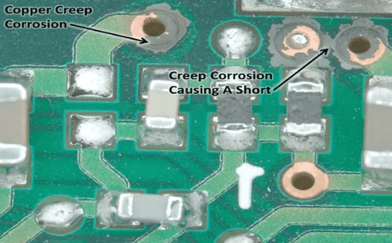
  • Grind away the surface layer to obtain the intermediate layer
  • Scan the intermediate layer to obtain a graphic file.
  • Repeat steps 2-4 until all layers are processed.
  • Use specialized software to convert the graphic file into an electrical file-the PCB diagram.If suitable software is available,the designer only needs to trace the diagram once.
  • Check and verify to complete the design.
Contact us for PCB quote now |

3.PCB Profiling Techniques

PCB profiling,especially multi-layer PCBs,is a time-consuming and laborious task involving a significant amount of repetitive work.Designers must be patient and meticulous,otherwise errors are easily made.The key to successful PCB profiling lies in using appropriate software to replace manual repetitive tasks,saving time and ensuring accuracy.

(1)Always use a scanner during profiling.

Many designers are accustomed to drawing lines directly on PCB design software such as proTel,padsor,or CAD.This is a very bad habit.The scanned graphic file serves as both the basis for converting to the PCB file and as a reference for subsequent verification.Using a scanner can significantly reduce the difficulty and intensity of labor.It’s no exaggeration to say that if a scanner is fully utilized,even someone without design experience can complete PCB profiling.

(2)Single-Direction Grinding.

Some designers, driven by speed, opt for bidirectional grinding (i.e., grinding away layers from the front and back surfaces toward the middle). This is a serious mistake. Bidirectional grinding can easily wear through, damaging other layers, with predictable consequences. Due to the manufacturing process and the presence of copper foil and pads, the outer layers of a PCB are the hardest, while the middle layers are the softest. Therefore, problems are most severe in the middle layers, often making them impossible to grind. Furthermore, PCB materials, hardness, and elasticity vary from manufacturer to manufacturer, making accurate grinding difficult.

(3)Choose excellent conversion software.

    Converting scanned graphics files to PCB files is crucial. With a good conversion file, designers can simply trace the graphics and complete the work. EDA2000 is highly recommended; it’s very convenient.

    The above are my personal thoughts, which I put forward for discussion, hoping to stimulate further discussion.

    Contact us for PCB quote now |
    Post Tags: #aluminum clad pcb#aluminum core pcb#aluminum pcb#assemble pcb

    Post navigation

    Previous Previous
    Design Tips for RF Circuit PCBs
    NextContinue
    The method of PCB power design

    Search

    Search

    Products

    • HDI Multilayer PCB
    • Rigid Flex PCB
    • Flex pcb
    • High Frequency PCB
    • High speed pcb
    • Heavy copper PCB
    • Metal Core PCB
    • Ceramic PCB

    Address

    Andwin Circuits Co.,Limited
    Email: sales@andwinpcb.com
    Tel: +86 755 2832 9394
    Fax:+86 755 2992  6717
    ADD:1-2F-1217,HouDeQun Industrial park,
    NanTing RD NO.56,ShaJing,BaoAn,Shenzhen 518104,GuangDong,China

    Products

    • HDI Multilayer PCB
    • Rigid Flex PCB
    • Flex pcb
    • High Frequency PCB
    • High speed pcb
    • Heavy copper PCB
    • Metal Core PCB
    • Ceramic PCB

    Technology

    • Blogs
    • Via in pad
    • PCB E-test
    • PCB stack up
    • Metal core PCB panelization
    • Controlled impedance PCB

    CERTIFICATION

    Certification >>


    Copyright© 2003 - 2026 Andwin | All Rights Reserved | Powered by Andwin

    Scroll to top
    • Home
    • Products
      • HDI multilayer PCB
      • Rigid Flex PCB
      • Flex pcb
      • Special PCB
        • High Frequency PCB
          • Rogers RO4350B PCB
          • Rogers RO4003 pcb
          • Rogers RO3003 PCB
          • Rogers 5880 PCB
          • DICLAD 527 PCB
          • Taconic TLX series
          • Taconic TLX-8 RF PCB
          • Taconic TLX-9 RF PCB
        • High speed pcb
          • Megtron 6 High Speed PCB
          • TU-872 SLK Sp High Speed
        • High TG PCB
          • SHENGYI SH260 PCB
          • ISOLA 370HR PCB
          • ISOLA IS410 PCB
          • ISOLA IS420 PCB
        • Heavy copper PCB
        • Copper coin pcb
        • Copper inlay PCB
      • Metal Core PCB
        • Copper core pcb
        • Aluminum PCB
        • 2 Layers Aluminum PCB
        • Direct thermal MCPCB
        • 2 Layers Direct Thermal
      • Ceramic PCB
        • DPC ceramic PCB
        • DBC ceramic PCB
        • Thick film Ceramic PCB
        • Al2O3 Alumina PCB
        • AIN ALN ceramic PCB
        • IGBT Ceramic PCB
    • Service
      • PCB Assembly
      • Quick turn PCB assembly
      • PCBA conformal coating
    • Industry
      • Telecommunication
      • IoT and Wireless
      • Industrial Control
      • Thermal management
      • Power and Energy
      • IC test board
      • Automative
      • Medical
    • Capability
      • Rigid PCB
      • Rigid flex PCB
      • Metal core PCB
      • PCB Assembly
    • Technology
      • Blogs
      • Via in pad
      • PCB E-test
      • PCB stack up
      • MCPCB panelization
      • Controlled impedance PCB
    • About
      • About us
      • Certification
      • Factory Tour
    • Contact
    Search