
Design Tips for RF Circuit PCBs
Because RF circuits are distributed parameter circuits,they are prone to skin effect and coupling effects in actual operation .Therefore ,in actual PCB design,interference radiation from these circuits is difficult to control.This includes interference between digital and analog circuits,power supply noise,and interference caused by improper grounding.Therefore,balancing the pros and cons of PCB design and finding the right compromise to minimize these interferences,or even eliminate interference from certain circuits,is crucial to the success of RF PCB design.This article provides some tips from a pcb layout perspective that will significantly help improve the anti-interference capabilities of RF circuits.
1.RF layout
Here,we discuss component layout should be arranged in straight line as much as possible,as shown in Figure 1.However,due to PCB and cavity space limitations,a straight line arrangement is often not possible .In such cases,an L-shaped layout can be used.A u-shaped layout(as shown in Figure2)is best avoided.When unavoidable,increase the distance between the input and output to at least 1.5cm.
The following techniques are commonly uesd in layout
1.1 Single-row Layout
The main RF signal components should be arranged in a straight line as much as possible,as shown in Figure 1.However ,due to PCB and cavity space limitations,a straight line arrangement is often not possible.In such case,an L-shaped layout can be used.A U-shaped layout(as shown in Figure2) is best avoided.When unavoidable,increase the distance between the input and output to at least 1.5cm.
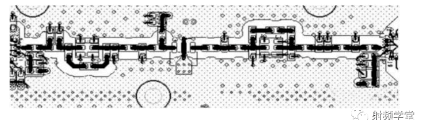
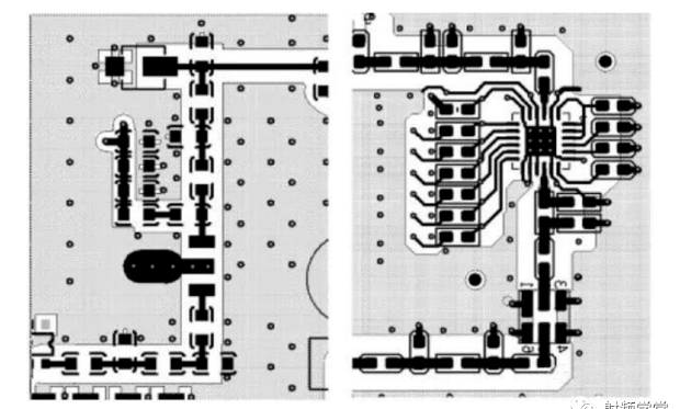
In addition,when using a an L-shaped or U-shaped layout ,the inflection point should not be curved immediately upon entering the interface,as shown in the left image of Figure3.Instead,it should be slightly straight,as shown in the right image of Figure 3.

1.2 Identical or Symmetrical Layout
Identical modules should be arranged in an identical or symmetrical layout whenever possible,as shown in Figures 4 and 5.
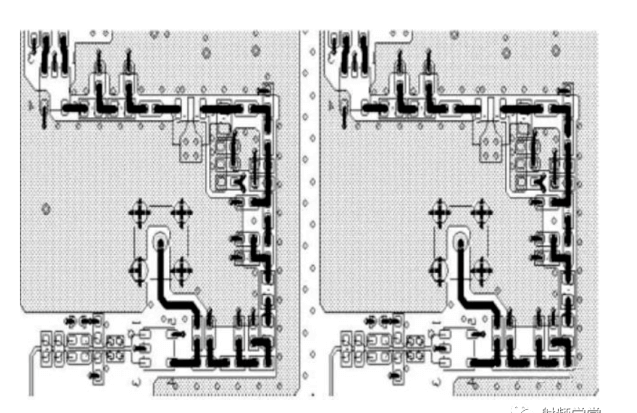
Figure 4 The same layout
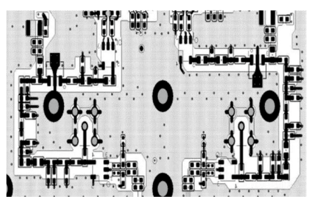
Figure 5 Symmetrical layout
1.3 Cross Layout
The bias circuit feed inductor is placed perpendicular to the RF path,as shown in Figure 6.primarily to avoid mutual inductance between inductors.
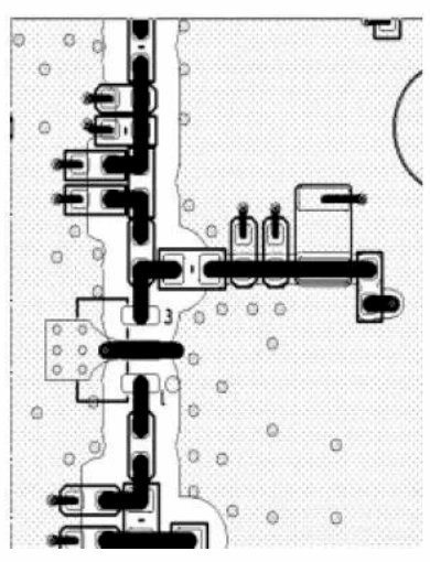
Figure 6 Cross figure
1.4 45° Layout
To optimize space utilization,components can be arranged at a 45-degree angle to keep RF traces as short as possible,as shown in Figure7.
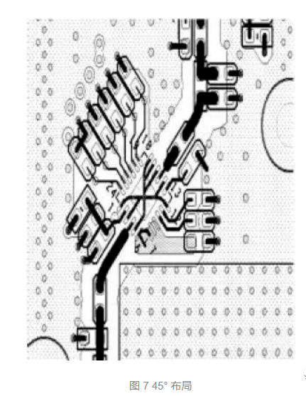
Figure 7 45° Layout
2.RF Routing
The overall routing requirements are:keep signal traces short and straight,minimize abrupt changes,minimize drilling ,avoid intersections with other signal traces,and add as many ground vias as possible around the RF signal traces.
The following are some common optimization method:
2.1 Gradient Line Processing
When the RF trace width is significantly larger than the IC device pin width,use a gradient width approach to the trace contacting the chip,as shown in Figure 8
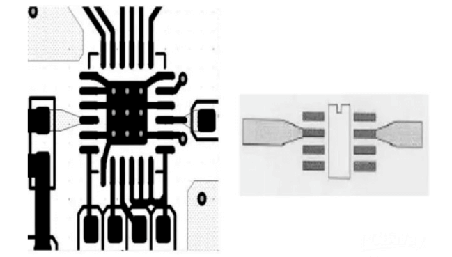
Figure 8 Gradient Line
2.2 Arc processing
If the RF line cannot be straight,treat it as an arc.This can reduce RF signal radiation and mutual coupling.Experiments have shown that bending the corners of the transmission line at right angles can minize return loss.This is shown in Figure 9.

2.3 Ground and Power Lines
Ground lines should be as thick as possible .If possible ,every layer of the PCB should be grounded,and the ground line should be connected to the main ground line.Provide sufficient ground vias to minimize ground impedance
The RF circuit power supply should not be split into separate planes.A full power plane not noly increases RF signal radiation but also makes it susceptible to interference from RF signals.Therefore,power lines or planes are generally long and processed according to the current flow.Thicken as much as possible while meeting the current capacity,but do not wide meeting the current capacity,but do not widen it indefinitely.When handing power lines,be sure to avoid loops.
The power and ground lines must run parallel to the direction of the RF signal,but they must not overlap.It’s best to use a vertical cross where a cross is available.
2.4 Crossover Handling
When possible,cross the RF ans IF signals with the ground plane.
When RF signals cross other signal traces,try to run a ground plane connected to the main ground plane along the RF traces between them.If this is not possible,ensure that they are crossed,Other signal traces here also include power lines.
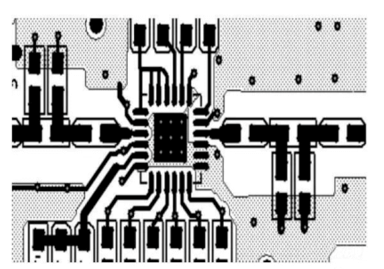
2.5 Coplanar Impedance
Coplanar impedance of important signals,such as RF signals,interference soures,and sensitive signal,can both improve the signal’s immunity to interference and reduce the signal’s interference with other signals.This is shown in Figure 10.
2.6 Copper Foil Processing
Copper foil must be smooth,with no long lines or sharp corners.If this is unavoidable,several ground vias should be placed around sharp corners,thin,elongated copper foil,or at the edges of the copper foil.
2.7 Spacing
RF traces must be at least 3W away from the edge of the adjacent ground layer,and no nonground vias should be within this 3W range.
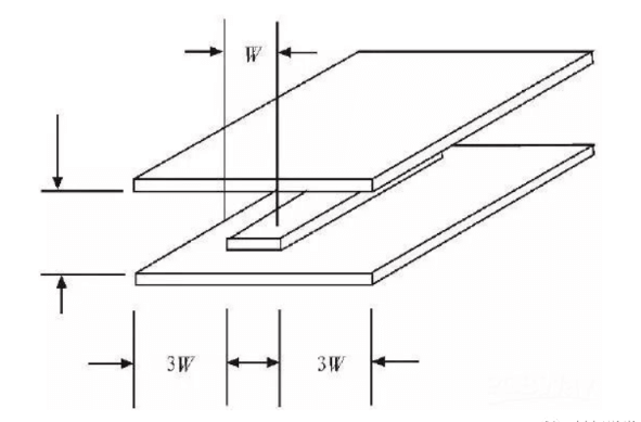
Figure 11 Spacing
RF traces on the same layer should have coplanar impedance,and ground vias should be added to the ground copper.The spacing between the vias should be less than1/20 of the wavelength(λ)corresponding to the signal frequency and should be evenly spaced.
3.Cavity Treatment
For the entire RF circuit,RF units in different modules should be isolated by cavities,especially between sensitive circuits and strong radiation sources.In high-power multistage amplifiers,isolation between stages must also be ensured.
After the circuit branches are laid out,the shield cavity must be prepared.The following points should be considered:
The corners of the shield cavity should be rounded.The metal shield cavity is typically cast.The curved corners facilitate mold removal during casting,as shown in Figure12.
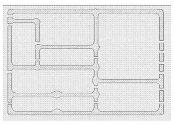
Figure 12 Type
The shield cavity is sealed from the outside,and the interface lines entering the cavity are typically stripline or microstrip lines.
3mm plated holes are placed at the corners of the cavity to secure the shield shell.Equally spaced holes are placed throughout each long cavity to provide enhanced support.
The cavity is usually windowed to facilitate soldering of the shield shell.The cavity is generally thicker than 2mm, and two rows of window screens are added within the cavity .Vias are staggered,and the distance between vias in the same row is 150mlil
4.Conclusion
In RF circuit PCB design,reducing circuit radiation and thus improving anti-interference capabilities are crucial.However,in actual layout and routing,some issues are often conflicding.Finding a compromise to optimize the overall performance of the entire RF circuit is a crucial consideration for designers.This article summarizes some design experiences that may help improve the anti-interference capabilities of RF circuit PCBs.We hope this will helpful to beginners in RF circuit design.