Skip to content
Andwin Circuits
  • Home
  • ProductsExpand
    • HDI multilayer PCB
    • Rigid Flex PCB
    • Flex pcb
    • Special PCBExpand
      • High Frequency PCBExpand
        • Rogers RO4350B PCB
        • Rogers RO4003 pcb
        • Rogers RO3003 PCB
        • Rogers 5880 PCB
        • DICLAD 527 PCB
        • Taconic TLX series
        • Taconic TLX-8 RF PCB
        • Taconic TLX-9 RF PCB
      • High speed pcbExpand
        • Megtron 6 High Speed PCB
        • TU-872 SLK Sp High Speed
      • High TG PCBExpand
        • SHENGYI SH260 PCB
        • ISOLA 370HR PCB
        • ISOLA IS410 PCB
        • ISOLA IS420 PCB
      • Heavy copper PCB
      • Copper coin pcb
      • Copper inlay PCB
    • Metal Core PCBExpand
      • Copper core pcb
      • Aluminum PCB
      • 2 Layers Aluminum PCB
      • Direct thermal MCPCB
      • 2 Layers Direct Thermal
    • Ceramic PCBExpand
      • DPC ceramic PCB
      • DBC ceramic PCB
      • Thick film Ceramic PCB
      • Al2O3 Alumina PCB
      • AIN ALN ceramic PCB
      • IGBT Ceramic PCB
  • ServiceExpand
    • PCB Assembly
    • Quick turn PCB assembly
    • PCBA conformal coating
  • IndustryExpand
    • Telecommunication
    • IoT and Wireless
    • Industrial Control
    • Thermal management
    • Power and Energy
    • IC test board
    • Automative
    • Medical
  • CapabilityExpand
    • Rigid PCB
    • Rigid flex PCB
    • Metal core PCB
    • PCB Assembly
  • TechnologyExpand
    • Blogs
    • Via in pad
    • PCB E-test
    • PCB stack up
    • MCPCB panelization
    • Controlled impedance PCB
  • AboutExpand
    • About us
    • Certification
    • Factory Tour
  • Contact
Andwin Circuits
Home / What details should be paid attention to in PCB design

What details should be paid attention to in PCB design

ByGrace July 9, 2025July 9, 2025

PCB design is complicated, and various unexpected factors will affect the achievement of the overall solution. In order to produce high-quality PCB boards on time, without increasing design time and incurring costly rework, design and circuit integrity problems must be discovered as early as possible in the design process.

However, there are many small details in the PCB design process. If some small details are not paid attention to, they may greatly affect the performance of the entire PCB and even determine the success or failure of the entire product. In order to maximize design efficiency and product quality, what other details should we pay attention to?

In the actual process of docking with customers, we have also summarized some precautions for character, appearance, and panel design. As a high-reliability multi-layer board manufacturer, Huaqiu Electronics focuses on PCB research and development and manufacturing, providing customers with a high-reliability, short-delivery board experience.

“Reducing costs and increasing efficiency for the electronics industry” is our mission. We are well aware that in the main production chain, although the design, development and design engineering costs of products do not account for a high proportion, they will have a great impact on the total cost. Given the importance of the product design stage to the quality and cost of the final product, the following article combines actual cases of character, shape, and panel design to share expert solutions for some problems in the design to help reduce costs and increase efficiency throughout the process.

01.Character design case 1: Character design standardization
Contact us for PCB quote now |

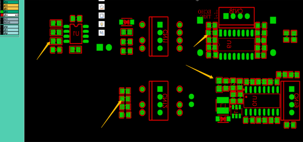
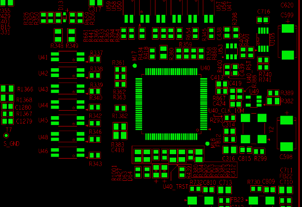
Problem: The industry generally uses machine stickers, and the requirements for logos are not high, but from an engineering perspective, the characters on the upper window pad will be judged as design abnormalities, which will take time to communicate back and forth.

Expert advice: For the convenience of maintenance and welding, place the bit number outside the device frame, and place or not place the bit number in the dense area in sequence.
02

Exterior design case 1: Considerations when designing the inner milling groove

Actual milling cutter access & production efficiency issues
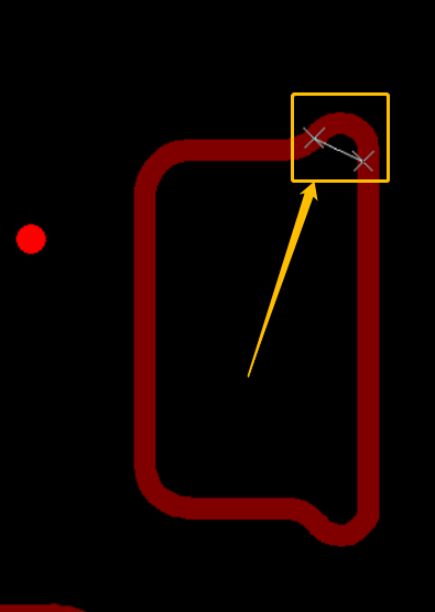
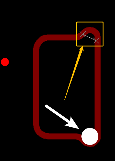
Problem: The design file provided by the customer requires the inner groove to be hollowed out, but the spacing at the arch is less than 0.8mm, and the conventional milling cutter cannot enter

Expert advice: When it does not affect the function of this board, it can be recommended that the customer increase the distance at the arc; place a “corner cleaning hole” at the concave corner (see the white arrow in the figure)
03

Exterior design case 2: Detailed design of board edge connection
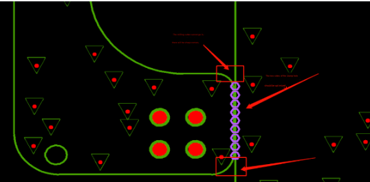
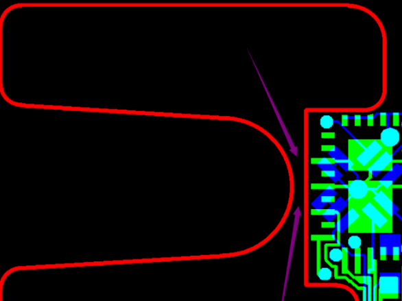
Problem: When designing the board edge connection, the two adjacent boards have rounded corners on one side and straight edges on the other side, and are connected by a stamp hole in the middle. When the milling cutter is used for cutting, sharp corners will be formed after the board is separated, and they need to be rounded after welding. The back-end processing method is generally to drill holes at both ends of the stamp hole. Drilling will cause slight damage to the board, which will generally affect the product, but in terms of PCB standards, it may cause disputes

Expert advice: Without affecting the structure, it is recommended to change the rounded corners to right angles or add “clearing corner holes” to increase production efficiency and make the board more beautiful.

04

SET panel design case 1: panel direction expression
Contact us for PCB quote now |

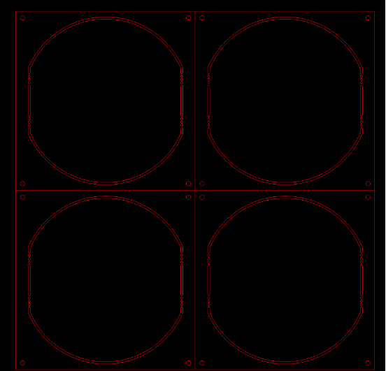
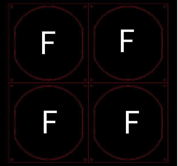
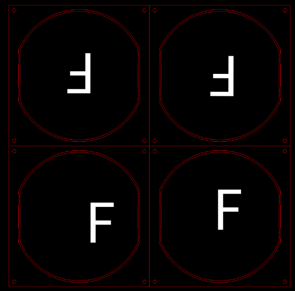
Problem: In the panel direction expression, the customer provides a completely symmetrical panel diagram similar to the left picture above, or provides a physical picture reference similar to the right picture above, without clearly indicating the panel direction. If the small device symbol in the middle is not carefully observed, it is difficult for the back-end personnel to know that it is a parallel panel, and it is easy to mistake it for a straight panel, resulting in interference of devices during welding and failure to weld.

Expert advice: From a standard perspective, clear direction identification is required on the design file (except for asymmetric files)
The above are several cases of PCB design detail optimization.

Contact us for PCB quote now |

Post Tags: #aluminum clad pcb#aluminum core pcb#aluminum pcb#assemble pcb#pcb design

Post navigation

Previous Previous
Solve EMI problems through high-speed PCB control
NextContinue
What are the causes of PCB failure?

Search

Search

Products

  • HDI Multilayer PCB
  • Rigid Flex PCB
  • Flex pcb
  • High Frequency PCB
  • High speed pcb
  • Heavy copper PCB
  • Metal Core PCB
  • Ceramic PCB

Address

Andwin Circuits Co.,Limited
Email: sales@andwinpcb.com
Tel: +86 755 2832 9394
Fax:+86 755 2992  6717
ADD:1-2F-1217,HouDeQun Industrial park,
NanTing RD NO.56,ShaJing,BaoAn,Shenzhen 518104,GuangDong,China

Products

  • HDI Multilayer PCB
  • Rigid Flex PCB
  • Flex pcb
  • High Frequency PCB
  • High speed pcb
  • Heavy copper PCB
  • Metal Core PCB
  • Ceramic PCB

Technology

  • Blogs
  • Via in pad
  • PCB E-test
  • PCB stack up
  • Metal core PCB panelization
  • Controlled impedance PCB

CERTIFICATION

Certification >>


Copyright© 2003 - 2026 Andwin | All Rights Reserved | Powered by Andwin

Scroll to top
  • Home
  • Products
    • HDI multilayer PCB
    • Rigid Flex PCB
    • Flex pcb
    • Special PCB
      • High Frequency PCB
        • Rogers RO4350B PCB
        • Rogers RO4003 pcb
        • Rogers RO3003 PCB
        • Rogers 5880 PCB
        • DICLAD 527 PCB
        • Taconic TLX series
        • Taconic TLX-8 RF PCB
        • Taconic TLX-9 RF PCB
      • High speed pcb
        • Megtron 6 High Speed PCB
        • TU-872 SLK Sp High Speed
      • High TG PCB
        • SHENGYI SH260 PCB
        • ISOLA 370HR PCB
        • ISOLA IS410 PCB
        • ISOLA IS420 PCB
      • Heavy copper PCB
      • Copper coin pcb
      • Copper inlay PCB
    • Metal Core PCB
      • Copper core pcb
      • Aluminum PCB
      • 2 Layers Aluminum PCB
      • Direct thermal MCPCB
      • 2 Layers Direct Thermal
    • Ceramic PCB
      • DPC ceramic PCB
      • DBC ceramic PCB
      • Thick film Ceramic PCB
      • Al2O3 Alumina PCB
      • AIN ALN ceramic PCB
      • IGBT Ceramic PCB
  • Service
    • PCB Assembly
    • Quick turn PCB assembly
    • PCBA conformal coating
  • Industry
    • Telecommunication
    • IoT and Wireless
    • Industrial Control
    • Thermal management
    • Power and Energy
    • IC test board
    • Automative
    • Medical
  • Capability
    • Rigid PCB
    • Rigid flex PCB
    • Metal core PCB
    • PCB Assembly
  • Technology
    • Blogs
    • Via in pad
    • PCB E-test
    • PCB stack up
    • MCPCB panelization
    • Controlled impedance PCB
  • About
    • About us
    • Certification
    • Factory Tour
  • Contact
Search