
When Should You Use HDI PCB Instead of Multilayer PCB?
Choosing between HDI (High-Density Interconnect) PCBs and traditional multilayer PCBs can significantly impact your product’s performance, size, and cost. While both technologies serve the electronics industry, understanding when to use each type is crucial for optimal design outcomes. This comprehensive guide will help you make informed decisions based on your specific project requirements.
Understanding HDI PCB and Multilayer PCB Basics
Before diving into when to use each technology, let’s establish a clear understanding of what HDI and multilayer PCBs actually are.
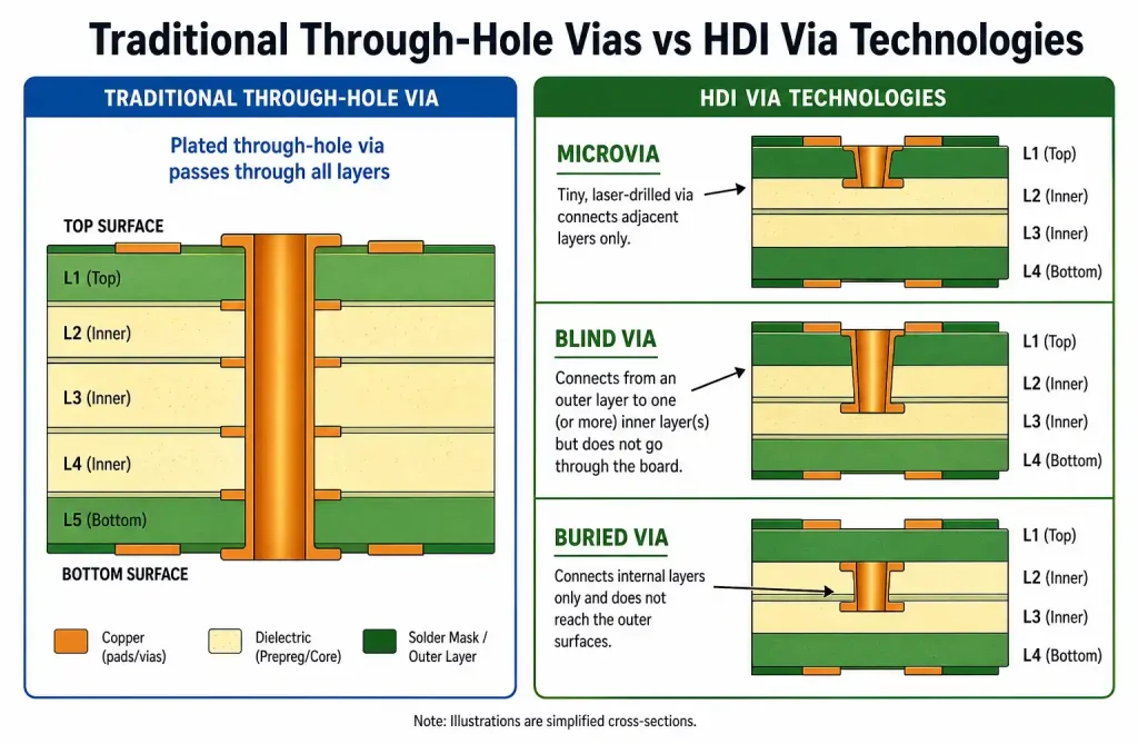
Multilayer PCBs are circuit boards with three or more conductive copper layers laminated together with insulating material. They’ve been the industry standard for decades, offering reliable performance for a wide range of applications. These boards use traditional through-hole vias to connect different layers.
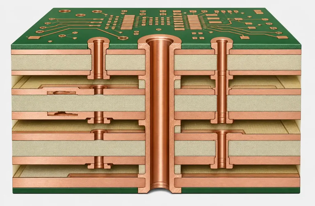
HDI PCBs represent an advanced evolution in PCB technology. They feature finer lines and spaces (typically less than 100 microns), smaller vias (microvia diameter less than 150 microns), and higher connection pad density. HDI boards use blind vias, buried vias, and microvias instead of traditional through-holes, allowing for more compact designs.
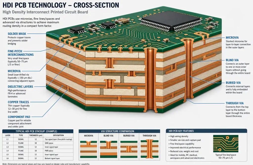
The fundamental difference lies in the interconnection density. HDI technology enables you to pack more functionality into a smaller footprint, which has become increasingly important as devices continue to shrink while demanding more features.
Key Differences Between HDI and Multilayer PCBs
Understanding the technical distinctions helps clarify when each technology excels.
Via Technology
Traditional multilayer PCBs primarily use through-hole vias that penetrate the entire board thickness. HDI PCBs employ microvias (typically 0.006″ or smaller), blind vias (connecting outer layers to inner layers), and buried vias (connecting only inner layers without reaching the surface).
Line Width and Spacing
Multilayer PCBs typically feature trace widths of 4-6 mils (0.1-0.15mm) or larger. HDI PCBs can achieve trace widths as fine as 2-3 mils (0.05-0.075mm) or even smaller, with correspondingly tighter spacing.
Layer Count and Thickness
While both can have multiple layers, HDI technology allows you to achieve the same functionality with fewer layers, or pack more functionality into the same layer count. HDI boards are generally thinner due to the use of thinner dielectric materials and smaller vias.
Component Density
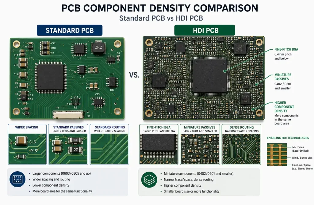
HDI PCBs support much higher component density, with the ability to accommodate fine-pitch BGAs (Ball Grid Arrays) with pitches of 0.5mm or less, and components with 0201 or 01005 package sizes.
When HDI PCB is the Right Choice
HDI technology shines in specific scenarios where its advanced capabilities justify the additional cost and complexity.
Space-Constrained Applications
If your product has strict size limitations, HDI is often the only viable solution. Smartphones, wearables, hearing aids, and other compact devices simply cannot accommodate traditional multilayer PCBs while maintaining required functionality.
High-Speed Signal Requirements
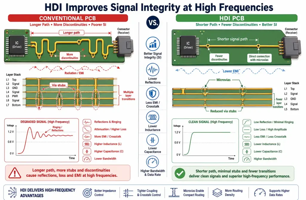
When dealing with high-frequency signals (above 1 GHz), HDI’s shorter signal paths and reduced via stubs significantly improve signal integrity. The smaller vias in HDI boards have lower inductance and capacitance, reducing signal degradation.
Fine-Pitch Component Integration
Modern processors, FPGAs, and memory chips often come in fine-pitch BGA packages with 0.5mm pitch or smaller. HDI technology provides the routing density needed to fan out these components effectively without requiring excessive layer counts.
Weight-Critical Designs
Aerospace, drone, and portable medical devices benefit from HDI’s lighter weight. By reducing layer count and overall board thickness, HDI can significantly decrease product weight.
High-Reliability Applications
The shorter interconnections in HDI boards mean fewer potential failure points. Medical implants, aerospace electronics, and military applications often specify HDI for enhanced reliability.
Advanced Functionality in Limited Space
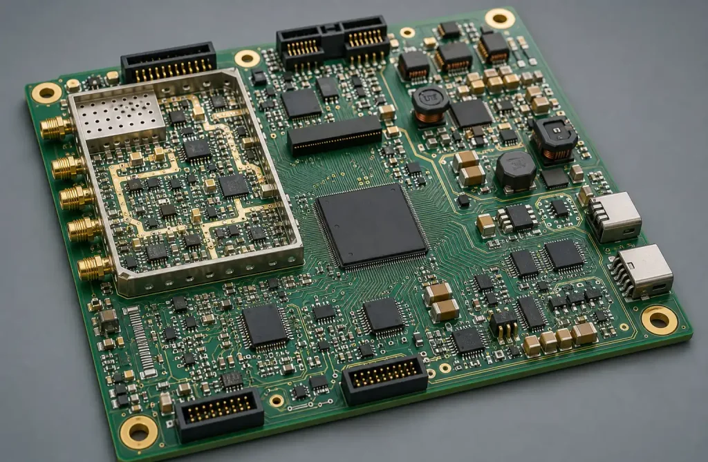
When you need to integrate multiple functions—such as RF, power management, and digital processing—into a compact form factor, HDI’s routing density makes it possible without compromising performance.
When Traditional Multilayer PCB Makes More Sense
Despite HDI’s advantages, traditional multilayer PCBs remain the better choice for many applications.
Cost-Sensitive Projects
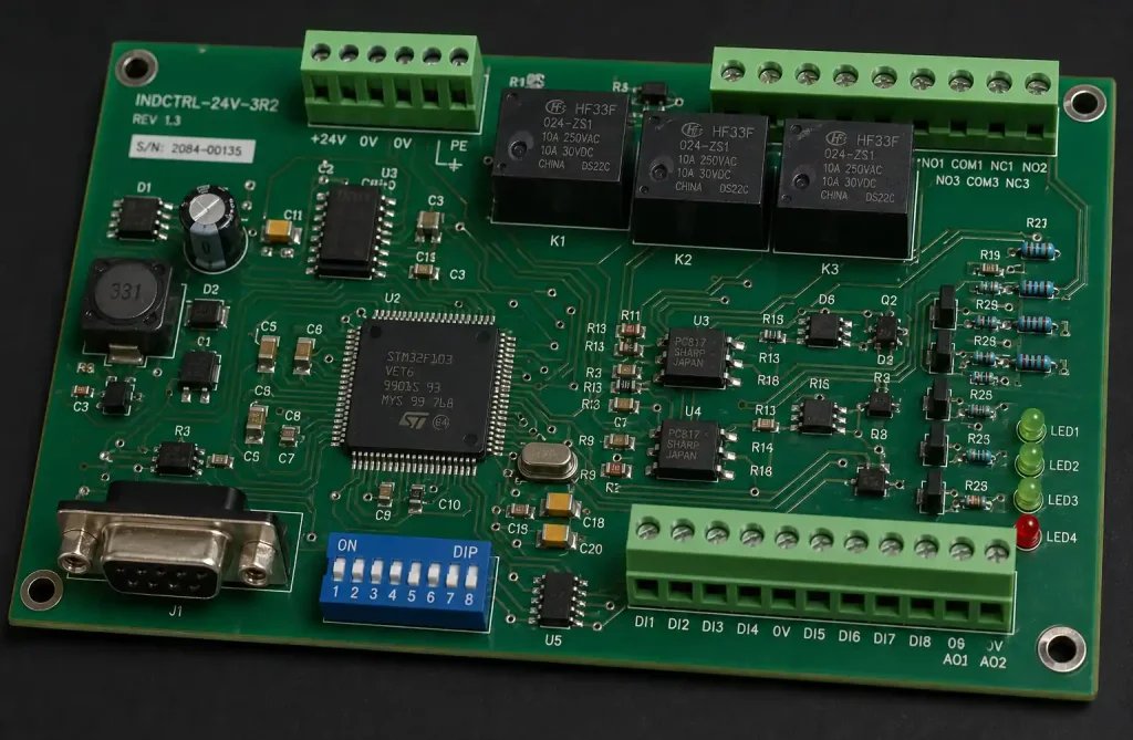
For consumer electronics, industrial controls, and other price-competitive markets, traditional multilayer PCBs offer excellent performance at a lower cost. If your design doesn’t require HDI’s advanced features, the extra expense isn’t justified.
Lower Component Density Designs
When using standard-pitch components (1.0mm BGA pitch or larger, 0402 or larger passives), traditional multilayer technology provides adequate routing capability without HDI’s complexity.
Simpler Signal Requirements
Applications operating at lower frequencies (below 500 MHz) with less demanding signal integrity requirements don’t benefit significantly from HDI’s advanced features.
Larger Form Factors
When board size isn’t constrained, traditional multilayer PCBs can achieve the same functionality as HDI at lower cost. Industrial equipment, server boards, and automotive control units often have sufficient space for conventional designs.
High-Power Applications
Power electronics, motor drives, and high-current applications benefit from the thicker copper and larger vias available in traditional multilayer construction. HDI’s fine features aren’t well-suited for high-power distribution.
Faster Time-to-Market
Traditional multilayer PCBs have shorter manufacturing lead times and broader manufacturer availability. If speed to market is critical and HDI features aren’t required, conventional technology accelerates your schedule.
Easier Rework and Repair
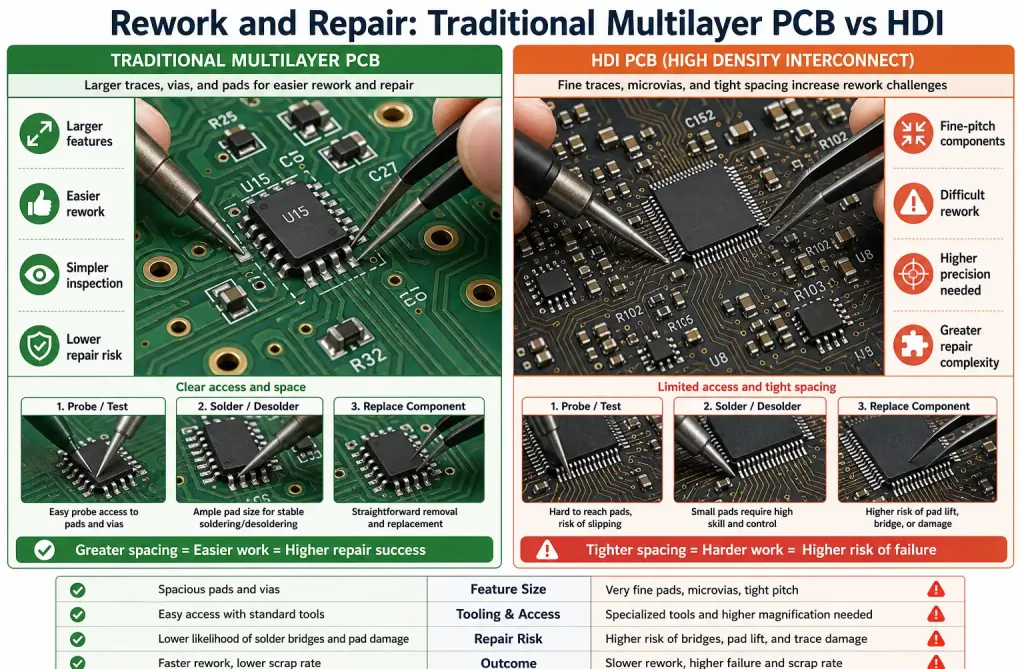
The larger features of traditional multilayer PCBs make them easier to rework, repair, and troubleshoot. This matters for prototyping, low-volume production, and field-serviceable products.
Cost Considerations: HDI vs Multilayer
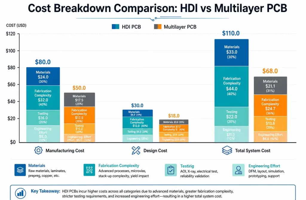
Cost differences between HDI and multilayer PCBs stem from multiple factors.
Manufacturing Costs
HDI PCBs typically cost 20-50% more than equivalent multilayer boards, sometimes even higher for advanced HDI designs. The premium comes from:
- Specialized equipment for laser drilling microvias
- More precise registration requirements
- Additional process steps (multiple lamination cycles)
- Higher scrap rates due to tighter tolerances
- Longer manufacturing cycles
Design Costs
HDI design requires more specialized expertise, potentially increasing engineering costs. However, this can be offset by reduced layer count and simplified routing.
Total System Cost
Consider the complete picture. HDI might enable:
- Smaller enclosures (reduced material costs)
- Fewer layers (partially offsetting HDI premium)
- Elimination of external components through better integration
- Reduced assembly costs due to smaller board size
Volume Considerations
At high volumes, HDI’s cost premium decreases as setup costs are amortized. For low-volume production, the percentage difference remains significant.
Break-Even Analysis
For many designs, there’s a crossover point where HDI becomes cost-effective despite higher PCB costs, typically when:
- Board size reduction exceeds 30-40%
- Layer count reduction is 2+ layers
- Component count decreases through better integration
- System-level costs (enclosure, assembly) decrease significantly
Performance Comparison
Performance differences between HDI and multilayer PCBs manifest in several key areas.
Signal Integrity
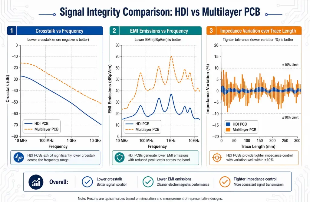
HDI’s shorter trace lengths and smaller vias reduce signal path inductance and capacitance, improving signal integrity at high frequencies. This translates to:
- Reduced crosstalk between adjacent traces
- Lower electromagnetic interference (EMI)
- Better impedance control
- Reduced signal reflections
Thermal Management
HDI’s thinner construction can present thermal challenges, but the technology also offers advantages:
- More efficient thermal via placement
- Better heat spreading through multiple thin layers
- Improved thermal coupling to components
Traditional multilayer boards with thicker copper layers may handle high-power applications better.
Electrical Performance
HDI boards typically exhibit:
- Lower parasitic capacitance and inductance
- Better power distribution through multiple thin power planes
- Reduced voltage drop across power distribution networks
- Improved grounding with more ground plane options
Reliability and Longevity
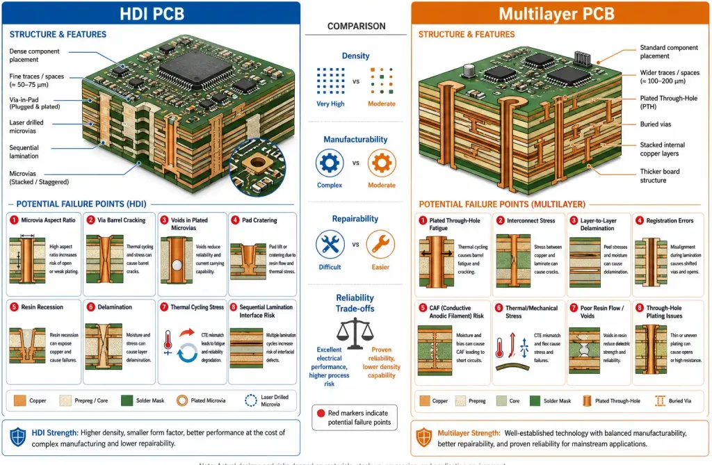
Both technologies offer excellent reliability when properly designed and manufactured. HDI’s shorter interconnections can reduce failure points, while traditional multilayer’s larger features may be more robust in harsh environments.
Manufacturing Complexity and Lead Times
Manufacturing considerations significantly impact project timelines and feasibility.
HDI Manufacturing Process
HDI fabrication involves:
- Sequential lamination (multiple press cycles)
- Laser drilling for microvias
- Precise layer-to-layer registration
- Specialized plating processes
- More rigorous inspection requirements
This complexity typically adds 1-2 weeks to lead times compared to traditional multilayer boards.
Manufacturer Capabilities
Not all PCB manufacturers can produce HDI boards. Advanced HDI designs may require:
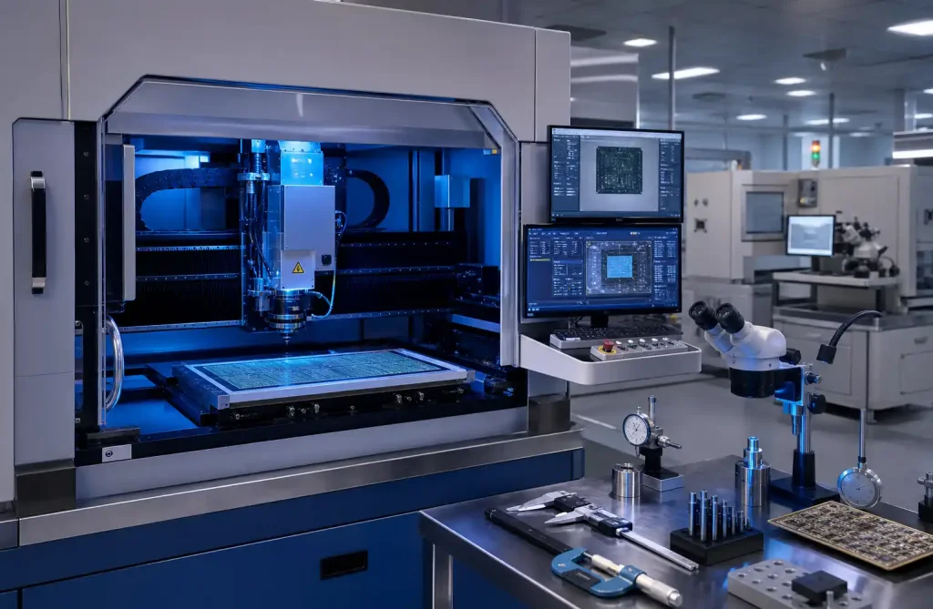
- Specialized facilities with laser drilling equipment
- Cleanroom environments
- Advanced inspection capabilities (X-ray, AOI)
- Experienced engineering support
Design for Manufacturing (DFM)
HDI designs require closer collaboration with manufacturers during the design phase. Early DFM reviews help avoid costly redesigns and ensure manufacturability.
Quality Control
HDI’s tighter tolerances demand more rigorous quality control, including:
- Microsectioning for via quality verification
- Impedance testing on every panel
- X-ray inspection for buried via integrity
- More extensive electrical testing
Industry Applications and Use Cases
Different industries favor HDI or multilayer PCBs based on their specific requirements.
HDI-Dominant Applications
Consumer Electronics: Smartphones, tablets, smartwatches, and wireless earbuds rely almost exclusively on HDI technology to achieve compact form factors with advanced functionality.

Medical Devices: Implantable devices, portable diagnostic equipment, and wearable health monitors use HDI for miniaturization and reliability.
Aerospace and Defense: Avionics, satellite systems, and military communications equipment leverage HDI for weight reduction and performance.
Automotive Advanced Systems: ADAS (Advanced Driver Assistance Systems), infotainment systems, and autonomous vehicle controllers increasingly adopt HDI technology.
Multilayer PCB-Dominant Applications
Industrial Controls: PLCs, motor drives, and industrial automation equipment typically use traditional multilayer PCBs for cost-effectiveness and robustness.
Power Electronics: Inverters, power supplies, and battery management systems benefit from multilayer’s ability to handle high currents.
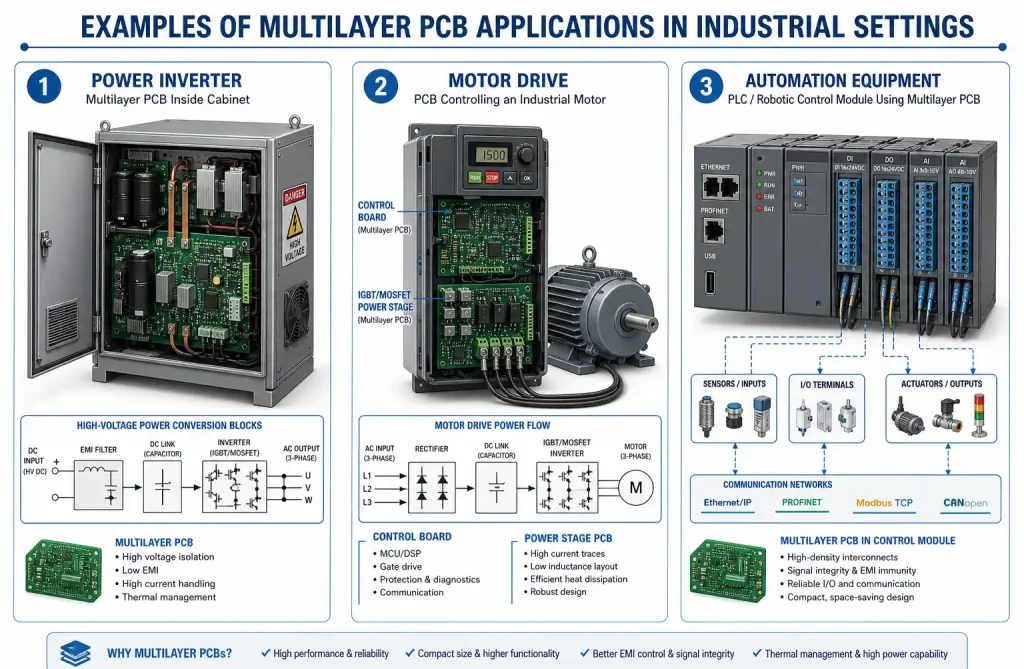
Telecommunications Infrastructure: Base stations, routers, and network switches often use traditional multilayer boards where size isn’t the primary constraint.
Automotive Traditional Systems: Engine control units, body control modules, and other standard automotive electronics continue using multilayer technology.
Hybrid Approaches
Some applications use both technologies:
- Main board: Traditional multilayer for cost
- Daughter cards: HDI for specific high-density functions
- Rigid-flex designs combining HDI and multilayer sections
Making the Final Decision
Choosing between HDI and multilayer PCBs requires evaluating multiple factors specific to your project.
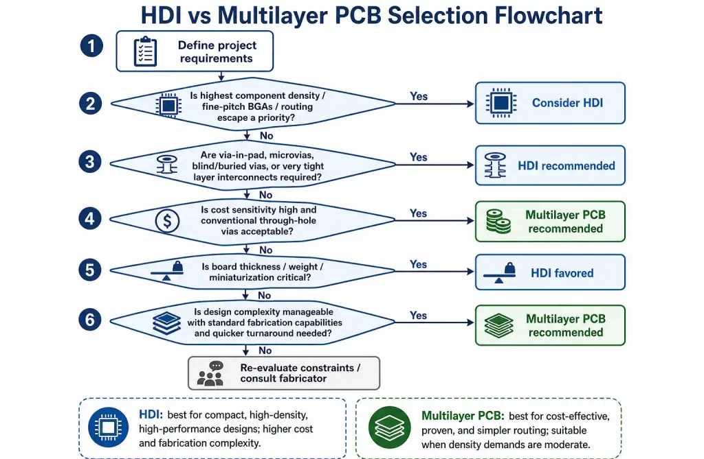
Decision Framework
Ask yourself these key questions:
Size Requirements
- Is board size strictly limited?
- Would a 30%+ size reduction provide significant value?
- Are there specific dimensional constraints?
Component Requirements
- What’s the finest component pitch?
- Are you using advanced BGAs or CSPs?
- What’s the required component density?
Performance Requirements
- What are the maximum signal frequencies?
- How critical is signal integrity?
- Are there specific impedance requirements?
Budget Constraints
- What’s the acceptable PCB cost per unit?
- What’s the production volume?
- What’s the total system cost impact?
Timeline Considerations
- What’s the required time-to-market?
- Can you accommodate longer lead times?
- Is manufacturer availability a concern?
Practical Decision Matrix
| Factor | Choose HDI When | Choose Multilayer When |
|---|---|---|
| Size | Space is critical | Adequate space available |
| Component Pitch | <0.5mm BGA pitch | >0.8mm pitch |
| Frequency | >1 GHz signals | <500 MHz |
| Volume | High volume (>10K) | Low-medium volume |
| Budget | Premium acceptable | Cost-sensitive |
| Timeline | Standard schedule | Urgent delivery |
Consulting with Manufacturers
Before finalizing your decision, consult with PCB manufacturers to:
- Verify design feasibility
- Get accurate cost quotes
- Understand lead time implications
- Identify potential design optimizations
Future Trends in PCB Technology
Understanding where PCB technology is heading helps inform long-term design decisions.
HDI Evolution
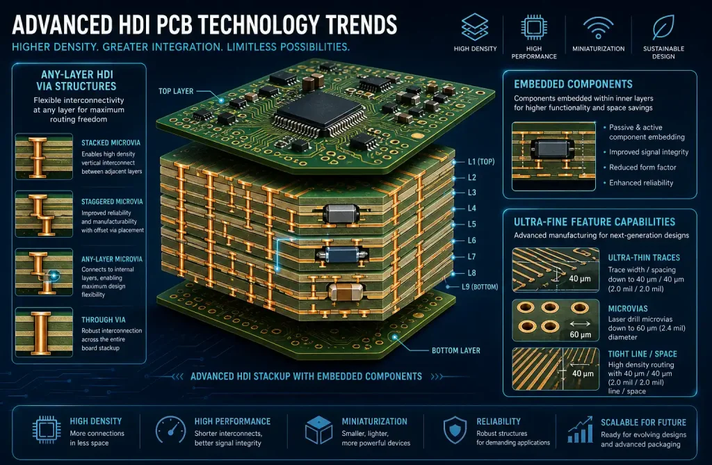
HDI technology continues advancing with:
- Any-layer HDI: Microvias connecting any layer to any other layer
- Finer features: Sub-2-mil traces and spaces becoming more common
- Advanced materials: Low-loss materials for 5G and beyond
- Embedded components: Passive components embedded within PCB layers
Multilayer Advancements
Traditional multilayer technology isn’t standing still:
- Improved materials: Better thermal performance and signal integrity
- Hybrid constructions: Combining thick and thin copper in single designs
- Enhanced manufacturing: Tighter tolerances at lower costs
- Larger formats: Supporting bigger boards for data centers and industrial applications
Convergence Trends
The line between HDI and advanced multilayer is blurring:
- Multilayer boards adopting some HDI features (blind/buried vias)
- HDI becoming more cost-competitive
- Hybrid designs combining both technologies
- Standardization of HDI processes reducing costs
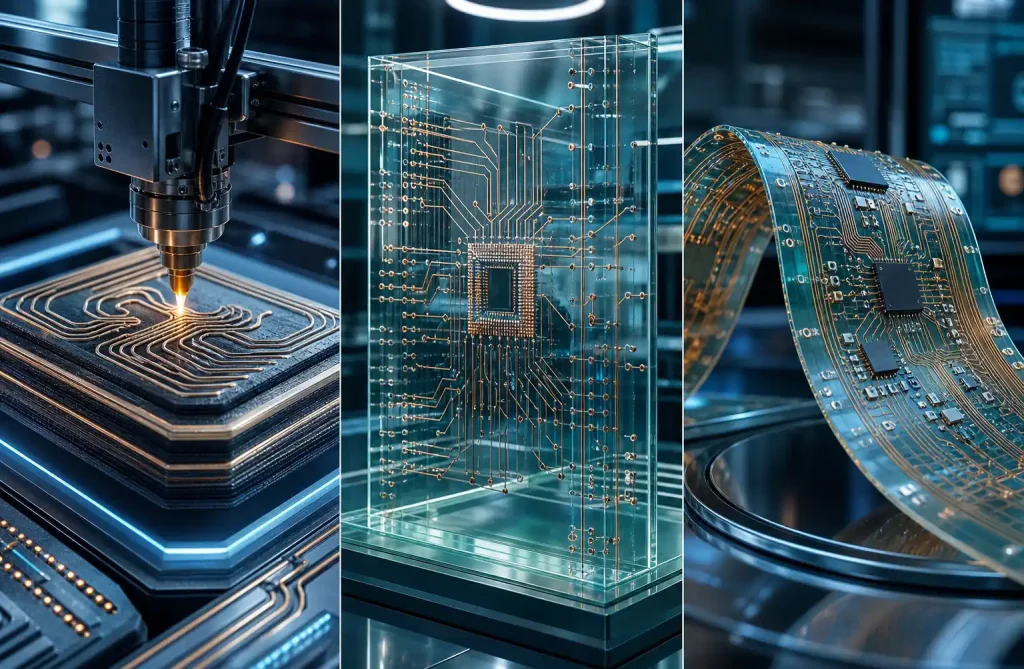
Emerging Technologies
Keep an eye on:
- 3D printed electronics: Additive manufacturing for PCBs
- Glass substrates: Ultra-fine features for next-generation devices
- Flexible and rigid-flex HDI: Combining flexibility with high density
- AI-assisted design: Optimizing HDI vs multilayer decisions automatically
Conclusion
The choice between HDI and multilayer PCBs isn’t about which technology is “better”—it’s about which is more appropriate for your specific application. HDI excels when miniaturization, high-speed performance, and advanced component integration are paramount, despite higher costs. Traditional multilayer PCBs remain the practical choice for cost-sensitive, larger form factor, or lower-frequency applications.
Evaluate your project requirements carefully, considering size constraints, component specifications, performance needs, budget, and timeline. When in doubt, consult with experienced PCB designers and manufacturers early in your design process. The right choice will optimize your product’s performance, cost, and time-to-market.
As technology evolves, HDI is becoming more accessible and cost-effective, gradually expanding into applications previously dominated by traditional multilayer boards. Staying informed about these trends will help you make better decisions for current and future projects.