
Flexible PCB Structure Explained: Substrate, Copper Foil, and Coverlay Layers
Flexible printed circuit boards (flex PCBs) have revolutionized modern electronics by enabling bendable, lightweight, and space-efficient circuit designs. Understanding the layered structure of flexible PCBs—particularly the substrate, copper foil, and coverlay—is essential for engineers, designers, and manufacturers working with this technology. This comprehensive guide breaks down each component and explains how they work together to create reliable flexible circuits.
What is a Flexible PCB?
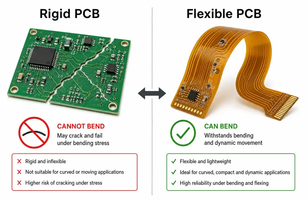
A flexible printed circuit board (flex PCB or FPC) is a type of electronic circuit constructed using flexible substrate materials that can bend, fold, and flex during use. Unlike rigid PCBs, flexible circuits can conform to three-dimensional shapes and withstand repeated flexing cycles, making them ideal for wearable devices, medical equipment, and aerospace applications.
The key advantage of flexible PCBs lies in their construction—thin, lightweight layers that maintain electrical performance while offering mechanical flexibility. This unique combination comes from carefully selected materials and precise manufacturing processes.
Core Components of Flexible PCB Structure
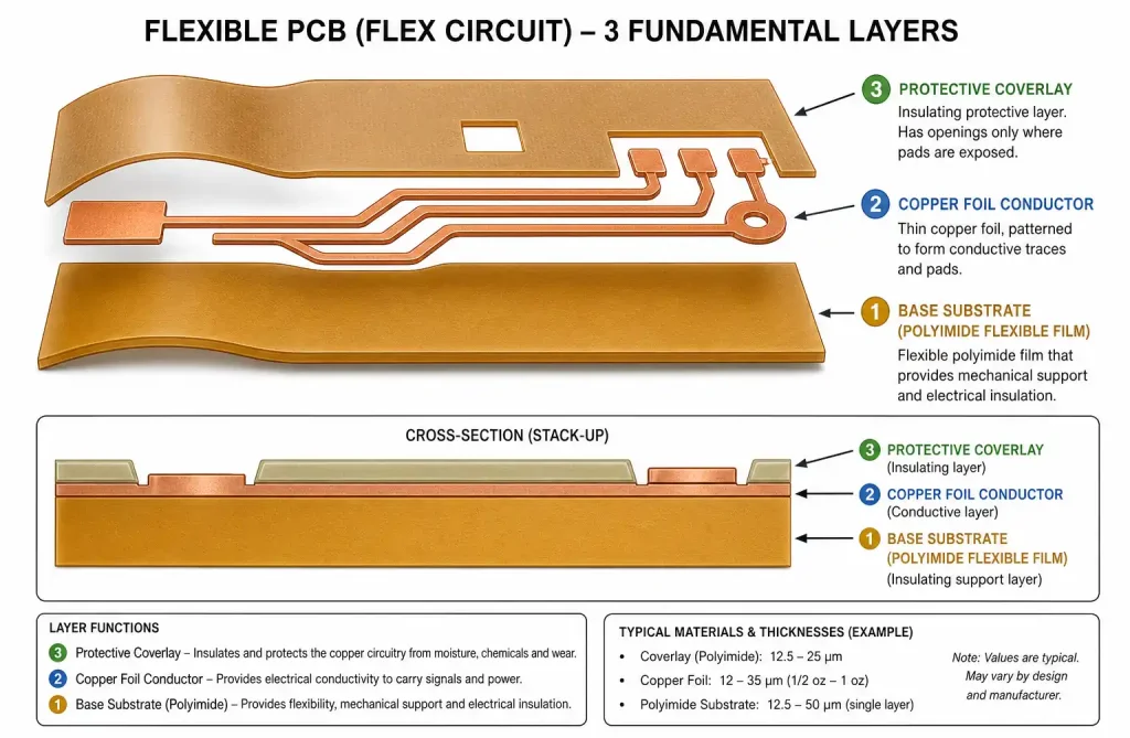
Every flexible PCB consists of three fundamental layers that work together to provide both electrical functionality and mechanical flexibility:
Base Substrate – The flexible dielectric material that forms the foundation of the circuit. This layer provides mechanical support and electrical insulation.
Copper Foil – The conductive layer that carries electrical signals. Copper traces are etched or deposited onto the substrate to create the circuit pattern.
Coverlay – The protective outer layer that insulates and protects the copper traces from environmental damage, oxidation, and mechanical wear.
Additional components may include adhesive layers, stiffeners, and surface finishes depending on the application requirements and design complexity.
The Substrate Layer: Foundation of Flexibility
The substrate is the backbone of any flexible PCB, providing both mechanical support and electrical insulation. Material selection for the substrate directly impacts the circuit’s flexibility, temperature resistance, and overall performance.
Polyimide (PI) Substrate
Polyimide is the most widely used substrate material for flexible PCBs, accounting for over 80% of flex circuit applications. This high-performance polymer offers exceptional properties:
- Temperature resistance: Operates continuously from -200°C to +400°C
- Chemical resistance: Withstands most solvents and chemicals
- Mechanical strength: High tensile strength and tear resistance
- Electrical properties: Excellent dielectric constant and low dissipation factor
- Dimensional stability: Minimal thermal expansion
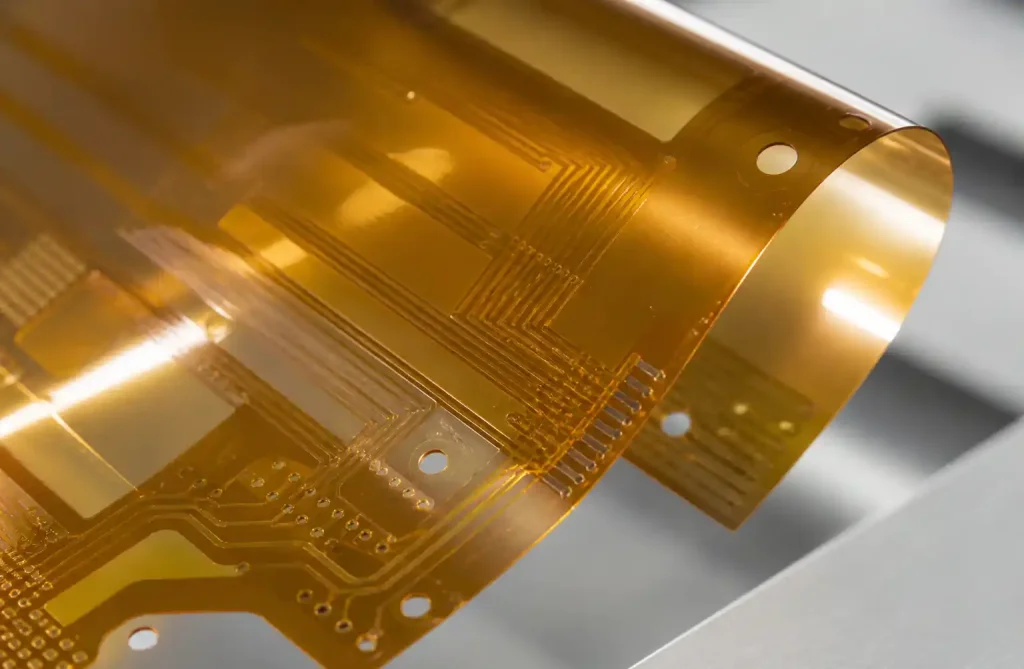
Common polyimide films include Kapton (DuPont), UPILEX (UBE), and Apical (Kaneka), with thicknesses typically ranging from 12.5μm to 125μm.
Polyester (PET) Substrate
Polyethylene terephthalate (PET) offers a cost-effective alternative for less demanding applications:
- Lower cost: 30-50% cheaper than polyimide
- Temperature range: -70°C to +150°C (limited compared to PI)
- Good flexibility: Suitable for static or low-flex applications
- Moisture resistance: Better moisture barrier than polyimide
PET substrates work well for consumer electronics, membrane switches, and applications without extreme temperature requirements.
Other Substrate Materials
Polyethylene Naphthalate (PEN) – Offers better temperature resistance than PET (up to 200°C) while maintaining cost advantages over polyimide.
Liquid Crystal Polymer (LCP) – Provides superior high-frequency performance, extremely low moisture absorption, and excellent dimensional stability for RF and microwave applications.
Copper Foil: The Conductive Pathway
Copper foil forms the conductive traces that carry electrical signals throughout the flexible PCB. The type, thickness, and bonding method of copper foil significantly affect circuit performance, flexibility, and reliability.
Types of Copper Foil
Rolled Annealed (RA) Copper
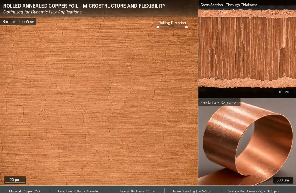
Rolled annealed copper is produced by mechanically rolling copper ingots into thin sheets. This process creates a grain structure that provides superior flexibility and fatigue resistance:
- Flexibility: Excellent for dynamic flex applications
- Bend cycles: Can withstand millions of flex cycles
- Surface: Smoother surface finish
- Cost: More expensive than electrodeposited copper
- Thickness range: Typically 9μm to 70μm
Electrodeposited (ED) Copper
Electrodeposited copper is created by electroplating copper onto a carrier foil. While less flexible than RA copper, it offers advantages for certain applications:
- Cost-effective: Lower manufacturing cost
- Fine features: Better for high-density circuits
- Thickness control: Precise thickness uniformity
- Applications: Best for static flex or rigid-flex designs
Copper Thickness Standards
Copper thickness is typically specified in ounces per square foot (oz/ft²) or micrometers (μm):
- ½ oz (18μm): Ultra-thin for maximum flexibility
- 1 oz (35μm): Standard thickness for most flex circuits
- 2 oz (70μm): Higher current capacity, reduced flexibility
Thinner copper provides better flexibility but limits current-carrying capacity. Engineers must balance electrical requirements with mechanical flexibility needs.
Copper Surface Treatment
The copper surface receives treatment to improve adhesion to the substrate:
- Oxide treatment: Creates a rough surface for mechanical bonding
- Brown oxide: Traditional treatment for adhesive-based systems
- Black oxide: Alternative treatment with different adhesion characteristics
Coverlay: Protection and Insulation
Coverlay is the protective layer applied over the copper traces to provide electrical insulation, environmental protection, and mechanical reinforcement. Proper coverlay selection and application are critical for long-term reliability.
Coverlay Materials
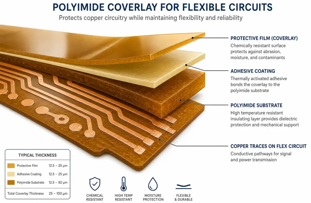
Polyimide Coverlay
The most common coverlay material consists of polyimide film with an adhesive layer:
- Material: Same polyimide as substrate for thermal compatibility
- Thickness: Typically 12.5μm to 50μm film + 15μm to 25μm adhesive
- Temperature rating: Matches substrate temperature range
- Flexibility: Maintains circuit flexibility
Photoimageable Coverlay (PSR)
Liquid photoimageable solder resist offers an alternative to traditional film coverlay:
- Application: Screen printed or curtain coated
- Fine features: Better resolution for small openings
- Thickness: Thinner than film coverlay (15-30μm)
- Cost: Lower material cost, higher processing cost
Coverlay Design Features
Openings and Windows
Coverlay includes precisely positioned openings for:
- Component pads: Expose copper for soldering components
- Test points: Allow electrical testing access
- Connectors: Provide contact areas for mating connectors
- Stiffener attachment: Enable bonding of rigid support areas
Registration Tolerance
Coverlay alignment to copper features requires tight tolerances:
- Standard tolerance: ±0.1mm to ±0.15mm
- Precision applications: ±0.05mm achievable with advanced processes
- Design rule: Minimum 0.15mm clearance between coverlay opening and copper edge
Coverlay Application Methods
Lamination Process
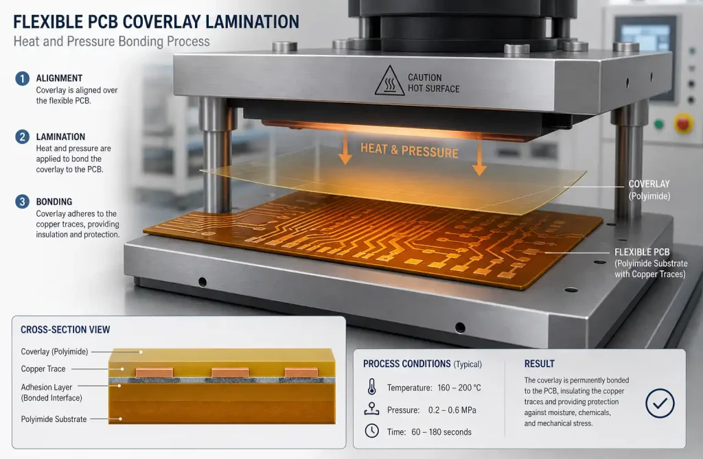
Traditional coverlay application uses heat and pressure:
- Align coverlay film over circuit
- Apply heat (typically 170-200°C)
- Apply pressure (300-400 PSI)
- Adhesive flows and bonds to substrate
Screen Printing
Liquid coverlay materials are screen printed:
- Print liquid material over circuit
- Expose through photomask
- Develop to remove unexposed areas
- Cure to final hardness
Adhesive Systems in Flexible PCBs
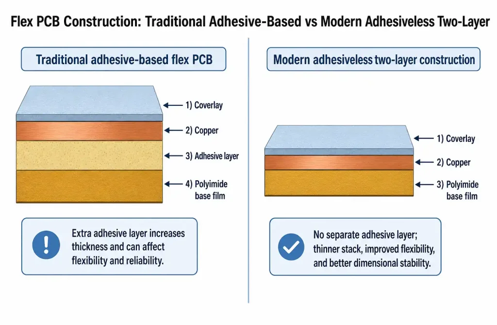
Adhesives bond the copper foil to the substrate and the coverlay to the circuit. The choice between adhesive and adhesiveless systems significantly impacts performance.
Adhesive-Based Construction
Traditional flex PCBs use acrylic or epoxy adhesives:
Advantages:
- Lower material cost
- Established manufacturing processes
- Good peel strength
- Suitable for most applications
Disadvantages:
- Increased total thickness
- Reduced flexibility
- Moisture absorption
- Outgassing at high temperatures
- Limited high-frequency performance
Adhesiveless Construction
Adhesiveless or “two-layer” flex PCBs eliminate the adhesive layer by directly bonding copper to polyimide:
Advantages:
- Thinner overall construction
- Better flexibility and bend radius
- Superior high-temperature performance
- Improved electrical properties at high frequencies
- No adhesive outgassing
- Better dimensional stability
Disadvantages:
- Higher material cost (15-30% premium)
- More complex manufacturing
- Requires specialized equipment
Manufacturing Methods:
- Cast method: Polyimide solution cast directly onto copper
- Sputtering: Thin metal layer sputtered, then copper plated
- Lamination: Special bonding without adhesive layer
Single-Layer vs Multi-Layer Flex PCB Construction
Flexible PCBs range from simple single-layer designs to complex multi-layer constructions with multiple copper layers.
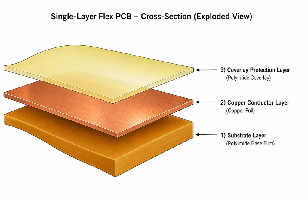
Single-Layer Flex PCB
The simplest construction consists of:
- One substrate layer
- One copper layer
- One or two coverlay layers (top and/or bottom)
Applications: Simple interconnects, membrane switches, basic sensors
Double-Sided Flex PCB
Adds copper on both sides of the substrate:
- One substrate layer
- Copper on both sides
- Plated through-holes for interlayer connection
- Coverlay on both sides
Applications: More complex circuits requiring higher density
Multi-Layer Flex PCB
Three or more copper layers with multiple substrate layers:
- Alternating substrate and copper layers
- Plated vias connecting layers
- Complex layer stackup design
- Outer coverlay protection
Applications: High-density circuits, impedance-controlled designs, complex routing
Rigid-Flex PCB
Combines rigid and flexible sections in one circuit:
- Rigid sections: Standard FR-4 PCB construction
- Flexible sections: Flex PCB construction
- Integrated design eliminates connectors
- Plated through-holes span rigid and flex areas
Applications: Devices requiring both rigid component mounting and flexible interconnection
Material Selection Considerations
Choosing the right materials for each layer requires balancing multiple factors:
Application Environment
Temperature Requirements
- Consumer electronics: PET acceptable (-40°C to +105°C)
- Automotive: Polyimide required (-55°C to +200°C)
- Aerospace: High-performance polyimide (-200°C to +400°C)
Chemical Exposure
- Polyimide: Excellent chemical resistance
- PET: Limited resistance to strong solvents
- LCP: Superior chemical resistance
Mechanical Requirements
Static Flex: Circuit bends during installation but remains stationary in use
- PET substrate acceptable
- ED copper suitable
- Standard adhesive systems work well
Dynamic Flex: Circuit flexes repeatedly during operation
- Polyimide substrate required
- RA copper essential
- Adhesiveless construction preferred
- Minimum bend radius: 10× total thickness
Flex-to-Install: Circuit flexes only during assembly
- PET or polyimide depending on temperature
- ED copper acceptable
- Cost-optimized materials
Electrical Performance
High-Frequency Applications
- LCP substrate for lowest loss
- Adhesiveless construction
- Controlled impedance design
- Smooth copper surface
High Current
- Thicker copper (2 oz or more)
- Wider traces
- Thermal management considerations
Cost Optimization
Material costs vary significantly:
- PET substrate: Lowest cost
- Polyimide with adhesive: Moderate cost
- Adhesiveless polyimide: Premium cost
- LCP substrate: Highest cost
Balance performance requirements against budget constraints by using premium materials only where necessary.
Manufacturing Process Overview
Understanding the manufacturing process helps designers create manufacturable flexible PCB designs.
Substrate Preparation
- Material inspection: Verify substrate quality and thickness
- Cleaning: Remove contaminants from substrate surface
- Copper lamination: Bond copper foil to substrate using heat and pressure
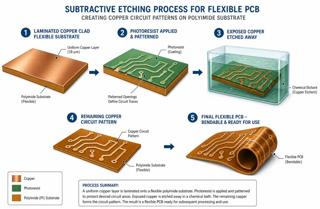
Circuit Patterning
Subtractive Process (most common):
- Apply photoresist to copper
- Expose through photomask
- Develop photoresist
- Etch away unprotected copper
- Strip remaining photoresist
Additive Process (for fine features):
- Deposit thin seed layer
- Pattern photoresist
- Electroplate copper in openings
- Remove photoresist and seed layer
Coverlay Application
- Alignment: Position coverlay over circuit
- Lamination: Apply heat and pressure
- Inspection: Verify coverlay registration
Drilling and Cutting
- Via drilling: Create holes for interlayer connections (multi-layer only)
- Plating: Electroplate through-holes
- Outline routing: Cut individual circuits from panel
Surface Finish
Apply protective finish to exposed copper:
- Electroless Nickel Immersion Gold (ENIG): Most common for flex
- Immersion Silver: Cost-effective alternative
- Immersion Tin: Good solderability
- Organic Solderability Preservative (OSP): Lowest cost
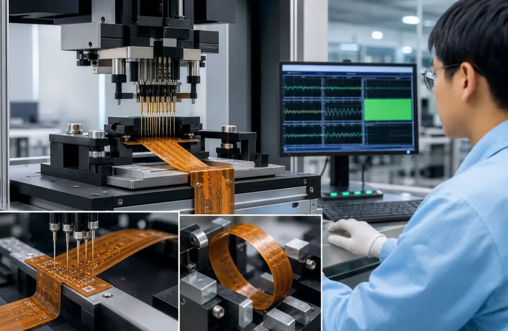
Final Inspection and Testing
- Visual inspection: Check for defects
- Electrical testing: Verify continuity and isolation
- Dimensional inspection: Confirm tolerances
- Flexibility testing: Verify bend performance
Common Applications and Use Cases
Flexible PCBs enable innovative designs across multiple industries:
Consumer Electronics
- Smartphones: Camera modules, display connections, battery interconnects
- Wearables: Fitness trackers, smartwatches, health monitors
- Laptops: Hinge connections, keyboard interconnects
Medical Devices
- Implantables: Pacemakers, cochlear implants, neurostimulators
- Diagnostic equipment: Ultrasound probes, endoscopes
- Wearable monitors: ECG patches, glucose monitors
Automotive
- Dashboard displays: Instrument clusters, infotainment systems
- Sensors: Airbag sensors, position sensors
- Lighting: LED arrays, adaptive headlights
Aerospace and Defense
- Avionics: Flight control systems, navigation equipment
- Satellites: Space-qualified flex circuits
- Military equipment: Ruggedized communications systems
Industrial
- Robotics: Joint interconnections, sensor arrays
- Test equipment: Probe cards, test fixtures
- Manufacturing: Automated assembly equipment
Quality Standards and Testing
Flexible PCBs must meet rigorous quality standards to ensure reliability:
Industry Standards
IPC-6013: Qualification and Performance Specification for Flexible Printed Boards
- Defines quality levels (Class 1, 2, 3)
- Specifies acceptance criteria
- Covers materials, construction, and testing
IPC-2223: Sectional Design Standard for Flexible Printed Boards
- Design guidelines and best practices
- Material selection guidance
- Construction recommendations
Testing Methods
Peel Strength Testing: Measures adhesion between layers
- Minimum: 0.7 N/mm for adhesive systems
- Minimum: 0.9 N/mm for adhesiveless systems
Flexibility Testing: Verifies bend cycle performance
- Static flex: 100-1,000 cycles
- Dynamic flex: 100,000+ cycles required
Thermal Cycling: Tests reliability under temperature extremes
- Typical: -55°C to +125°C
- Aerospace: -200°C to +200°C
Electrical Testing: Confirms circuit integrity
- Continuity testing
- Isolation testing
- Impedance testing (controlled impedance designs)
Future Trends in Flexible PCB Materials
The flexible PCB industry continues to evolve with new materials and technologies:
Advanced Substrate Materials
Ultra-Thin Polyimide: Films as thin as 7.5μm enable even more flexible designs while maintaining electrical performance.
Transparent Flexible Substrates: Enable integration with displays and optical systems for augmented reality and transparent electronics.
Stretchable Substrates: Experimental materials that can stretch as well as bend, opening new application possibilities in wearables and soft robotics.
Improved Copper Technologies
Nano-Copper Inks: Printed copper traces offer lower-cost manufacturing for simple circuits.
Ultra-Thin Copper: Sub-9μm copper foils provide extreme flexibility while maintaining adequate conductivity for low-current applications.
Environmental Considerations
Halogen-Free Materials: Growing demand for environmentally friendly materials that meet RoHS and REACH requirements.
Recyclable Constructions: Development of flexible PCBs designed for easier end-of-life recycling.
Manufacturing Innovations
Roll-to-Roll Processing: Continuous manufacturing processes reduce costs for high-volume production.
Laser Direct Imaging: Eliminates photomasks for faster prototyping and lower setup costs.
3D Printed Flex Circuits: Additive manufacturing techniques enable rapid prototyping and custom geometries.
Conclusion
Understanding the structure of flexible PCBs—from the substrate foundation through the copper conductors to the protective coverlay—is essential for designing reliable, high-performance flexible circuits. Each layer plays a critical role in the overall performance, and material selection must balance electrical requirements, mechanical demands, environmental conditions, and cost constraints.
As technology advances, new materials and manufacturing processes continue to expand the capabilities of flexible PCBs, enabling increasingly sophisticated applications in consumer electronics, medical devices, automotive systems, and beyond. By mastering the fundamentals of flexible PCB structure, engineers and designers can create innovative solutions that leverage the unique advantages of this versatile technology.
Whether you’re designing a simple single-layer interconnect or a complex multi-layer rigid-flex assembly, understanding how substrate, copper foil, and coverlay work together provides the foundation for successful flexible PCB design and manufacturing.