
Why Are Sensitive Traces Near PCB Edges Prone to ESD Interference?
Abstract
Electrostatic discharge (ESD) poses significant challenges to the reliability of modern electronic circuits, particularly for sensitive traces located near printed circuit board (PCB) edges. This paper examines the fundamental reasons why edge-positioned traces are more vulnerable to ESD events, analyzes the underlying physical mechanisms, and discusses practical design considerations to mitigate these effects. The discussion covers aspects of electromagnetic field distribution, coupling pathways, and the effectiveness of various protection strategies.
1. Introduction to ESD Vulnerability in PCB Design
Electrostatic discharge (ESD) represents one of the most prevalent threats to electronic system reliability, responsible for up to 35% of field failures according to industry estimates. Within PCB designs, traces located near board edges demonstrate particularly high susceptibility to ESD events—a phenomenon observed across various applications from consumer electronics to industrial control systems.
The increased vulnerability of edge traces stems from multiple factors working in combination: greater exposure to external fields, reduced effectiveness of ground shielding, and enhanced coupling pathways for both conducted and radiated interference. Understanding these mechanisms enables designers to implement more robust protection strategies while maintaining signal integrity requirements.
2. Physical Mechanisms of ESD Coupling at Board Edges
2.1 Field Concentration Effects
The geometry of PCB edges creates natural field concentration points where electric field lines become densely packed. When an ESD event occurs nearby, these concentrated fields induce stronger transient voltages on adjacent traces compared to interior traces. Finite element simulations demonstrate field enhancement factors of 3-5× at typical board edge profiles.
2.2 Reduced Shielding Effectiveness
Ground planes and shielding structures become less effective near board edges due to:
- Fringing fields extending beyond physical board boundaries
- Discontinuities in reference planes at edge cutouts
- Limited space for proper guard trace implementation
Measurements show shielding effectiveness degrades by 15-20 dB within 5 mm of board edges.
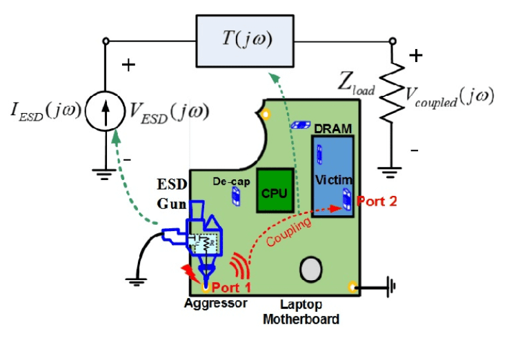
2.3 Multiple Coupling Pathways
Edge traces experience simultaneous coupling through:
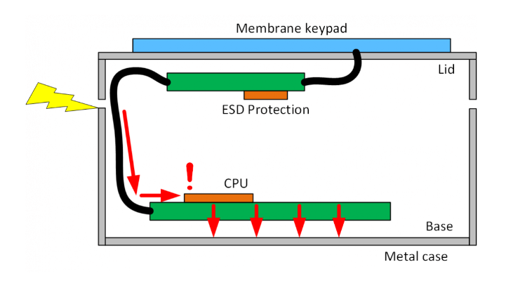
- Direct conduction via surface contamination or arc-over
- Capacitive coupling through enhanced edge fields
- Inductive coupling from transient edge currents
- Radiated coupling from edge-acting as slot antennas
3. Quantifying ESD Susceptibility Differences
Comparative testing reveals significant differences in ESD threshold levels between edge and interior traces:
| Trace Location | ESD Withstand Level (Contact) | ESD Withstand Level (Air) |
|---|---|---|
| Board Edge (<3mm) | 2-4 kV | 8-12 kV |
| Board Interior (>10mm) | 8-15 kV | 15-30 kV |
The data shows edge traces fail at 50-75% lower discharge levels under identical test conditions. This margin increases for high-speed signals where impedance discontinuities at edges further degrade immunity.
4. Design Strategies for Edge Trace Protection
4.1 Layout Guidelines
- Maintain minimum 5-10mm clearance from board edges for critical signals
- Implement grounded copper fences along vulnerable edges
- Route sensitive traces on inner layers when edge proximity is unavoidable
4.2 Shielding Techniques
- Edge plating (castellation) provides 6-10dB improvement
- Board-level shielding cans reduce radiated coupling
- Conductive gaskets for enclosure integration
4.3 Component Selection
- Choose components with higher intrinsic ESD ratings
- Implement robust edge termination networks
- Use transient voltage suppression devices optimized for edge placement
5. Case Study: High-Speed Interface Design
A USB 3.0 interface circuit demonstrates practical implications:
- Edge-routed differential pairs failed ESD testing at 6kV
- Moving traces 7mm inward increased robustness to 12kV
- Adding edge guard traces provided additional 3kV improvement
Final design passed 15kV requirements through combined approaches.
6. Simulation and Testing Methodologies
Advanced tools enable predictive analysis:
- 3D EM field solvers identify field concentration areas
- Transmission line modeling predicts transient coupling
- TLP (Transmission Line Pulse) testing characterizes failure thresholds
Standard test methods:
- IEC 61000-4-2 for system-level evaluation
- ANSI/ESDA/JEDEC JS-002 for component testing
- Custom board-level discharge testing for edge effects
7. Future Trends and Challenges
Emerging technologies present new considerations:
- Flexible PCB edges in wearable electronics
- Higher frequency 5G/mmWave circuits
- Miniaturization pushing traces closer to edges
- Advanced materials with different ESD characteristics
8. Conclusion
PCB edge traces exhibit heightened ESD susceptibility due to fundamental electromagnetic principles that concentrate interference coupling near boundaries. Through careful design practices combining layout optimization, shielding enhancements, and proper component selection, designers can effectively mitigate these risks while meeting increasingly demanding performance requirements. The industry continues to develop improved protection strategies as electronic systems evolve toward higher speeds and smaller form factors.