
Why Should Capacitors Be Placed Close to Components in PCB Design?
Introduction
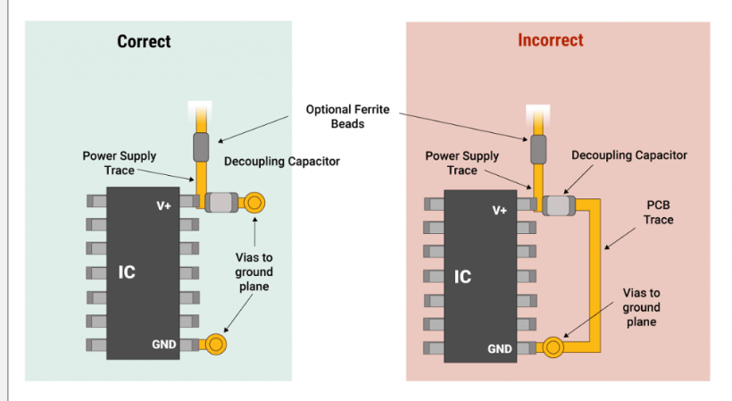
In printed circuit board (PCB) design, the placement of decoupling and bypass capacitors is a critical factor that directly impacts the performance, stability, and reliability of electronic circuits. One of the most fundamental rules in PCB layout is that capacitors—especially high-frequency decoupling capacitors—should be placed as close as possible to the power pins of integrated circuits (ICs) and other active components.
This article explores the reasons behind this design principle, covering key concepts such as parasitic inductance, high-frequency noise suppression, power integrity, and signal integrity. By understanding these factors, PCB designers can optimize their layouts for better performance and reduced electromagnetic interference (EMI).
1. The Role of Capacitors in PCB Design
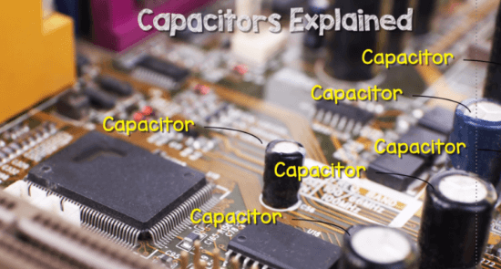
Capacitors serve multiple functions in electronic circuits, including:
- Decoupling (Bypassing): Providing a local energy reservoir to stabilize voltage levels by filtering high-frequency noise.
- Bulk Energy Storage: Supplying instantaneous current demands when ICs switch states.
- Filtering: Blocking unwanted AC signals while allowing DC to pass.
- Coupling/DC Blocking: Allowing AC signals to pass while blocking DC components.
Among these roles, decoupling capacitors are the most critical in high-speed digital and analog designs, where fast-switching ICs demand stable power delivery.
2. Why Should Capacitors Be Placed Close to Components?
2.1 Minimizing Parasitic Inductance
Every PCB trace and component lead has a small but non-negligible amount of parasitic inductance. The inductance ((L)) of a trace can be approximated by:
[
L \approx 5.08 \times 10^{-9} \times l \times \left( \ln \left( \frac{2l}{w + t} \right) + 0.5 + 0.2235 \frac{w + t}{l} \right)
]
Where:
- (l) = length of the trace (in inches)
- (w) = width of the trace (in inches)
- (t) = thickness of the trace (in inches)
Implications:
- Longer traces increase inductance, reducing the capacitor’s effectiveness at high frequencies.
- The impedance ((Z)) of an inductor increases with frequency ((f)):
[Z_L = 2 \pi f L]
At high frequencies, this impedance can dominate, preventing the capacitor from effectively suppressing noise.
Solution:
By placing the capacitor as close as possible to the IC’s power pin, the loop area between the IC, capacitor, and ground is minimized, reducing parasitic inductance.
2.2 Maintaining Power Integrity (PI)
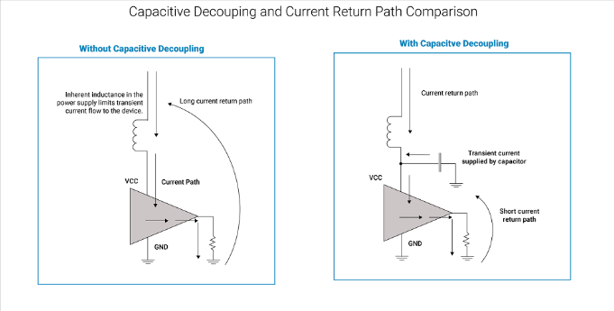
Power integrity refers to the stable and clean delivery of DC voltage to all components on a PCB. When an IC switches states, it draws sudden bursts of current, causing voltage droops (also called ground bounce or simultaneous switching noise, SSN).
How Capacitors Help:
- Decoupling capacitors act as local energy reservoirs, supplying instantaneous current.
- If the capacitor is too far away, the inductance of the trace delays the current delivery, leading to voltage fluctuations.
Example:
A 0.1 µF ceramic capacitor placed 1 mm away from an IC’s power pin will respond much faster than one placed 10 mm away due to lower inductance.
2.3 High-Frequency Noise Suppression
Modern digital ICs (e.g., CPUs, FPGAs, and high-speed memory) operate at GHz frequencies, generating fast transient currents. A capacitor’s effectiveness diminishes as frequency increases due to parasitic effects.
Key Points:
- Self-Resonant Frequency (SRF): Every capacitor has an SRF, beyond which it behaves like an inductor.
- Capacitor Placement Affects SRF: Longer traces add inductance, lowering the effective SRF.
Solution:
Using multiple capacitors (e.g., 0.1 µF, 1 µF, 10 µF) in parallel and placing them close to the IC ensures a low-impedance path across a wide frequency range.
2.4 Reducing Electromagnetic Interference (EMI)
Large current loops act as antennae, radiating EMI. If a decoupling capacitor is placed far from an IC, the loop area increases, leading to:
- Radiated emissions (violating FCC/CE regulations).
- Susceptibility to external noise (degrading signal integrity).
Solution:
Minimizing the loop area by placing capacitors close to ICs reduces EMI.
2.5 Signal Integrity (SI) Considerations
Noise on power rails can couple into signal traces, causing:
- Crosstalk (unwanted signal coupling).
- Jitter (timing errors in high-speed signals).
- False triggering (in analog/digital circuits).
Solution:
Proper decoupling near noise-sensitive components (e.g., ADCs, oscillators) ensures cleaner power delivery, improving signal integrity.
3. Best Practices for Capacitor Placement
To maximize the benefits of decoupling capacitors, follow these guidelines:
- Place the Smallest Capacitor Closest to the IC:
- High-frequency (0.1 µF, 0.01 µF) capacitors should be nearest to the power pin.
- Larger bulk capacitors (10 µF, 100 µF) can be slightly farther but still within a few millimeters.
- Use Multiple Vias for Low Inductance:
- Connect capacitors to ground/power planes with multiple vias to reduce impedance.
- Minimize Trace Length:
- Avoid long traces between the IC and capacitor.
- Follow Manufacturer Recommendations:
- Some IC datasheets specify exact decoupling requirements.
- Use a Solid Ground Plane:
- Ensures a low-impedance return path for high-frequency currents.
4. Real-World Example: Decoupling in a BGA Package
Ball Grid Array (BGA) packages have dense power and ground pins, making decoupling challenging. Poor placement can lead to:
- Voltage drops (due to high inductance).
- Resonances (causing power supply oscillations).
Solution:
- Use embedded capacitors (if possible).
- Place decoupling capacitors on the opposite side of the board directly under the BGA.
5. Conclusion
The rule of placing capacitors as close as possible to IC power pins is rooted in fundamental electrical principles: minimizing parasitic inductance, maintaining power integrity, suppressing high-frequency noise, reducing EMI, and improving signal integrity.
By adhering to best practices in capacitor placement, PCB designers can ensure stable, high-performance circuits that meet stringent industry standards. Whether designing high-speed digital boards or sensitive analog systems, proper decoupling is a small but crucial step that significantly impacts overall functionality.