
50-Layer PCB Manufacturing: Capabilities and Applications
When you design 5G base stations, phased array radar, or AI compute systems, standard boards hit routing limits around 12-16 layers. Beyond that, you need ultra-high layer count PCBs—30, 40, or 50 layers—to handle complex signal routing, power distribution, and ground planes that high-performance electronics demand.
Fifty-layer boards represent the extreme edge of FR-4 fabrication technology. They appear in telecommunications infrastructure, military radar, aerospace avionics, and computing hardware where signal integrity at multi-gigahertz frequencies and thousands of interconnects exceed standard capabilities.
This guide covers manufacturing capabilities, technical challenges, cost factors, and applications where 50-layer construction becomes necessary.
What Makes 50-Layer Manufacturing Different
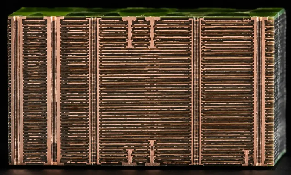
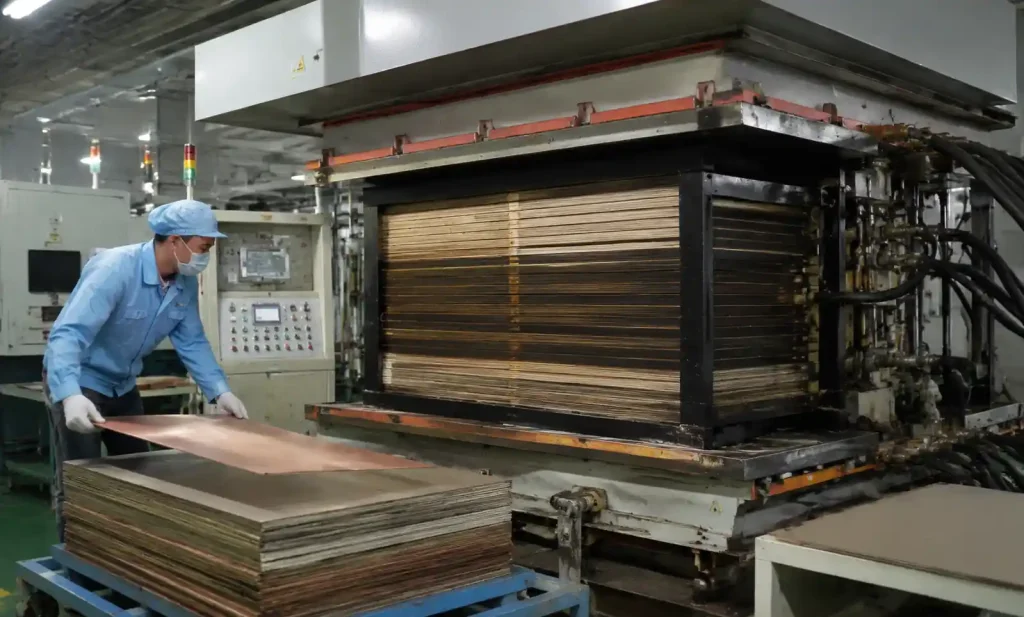
A 50-layer PCB requires sequential lamination of 24 core pairs with prepreg between them, creating 6-8mm finished thickness. Standard 12-layer boards are 1.6mm. This multiplication creates complex manufacturing challenges.
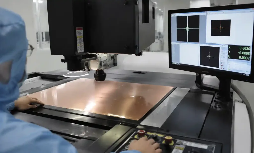
The core challenge is layer-to-layer registration accuracy. When your board has microvias connecting layers 1-2, blind vias to layer 15, and buried vias between layers 20-25, registration error of 50 microns causes failures. Andwin Circuits’ PCB manufacturing uses optical alignment systems with ±25μm tolerance to prevent these issues.
Sequential lamination means 3-5 press cycles versus one for standard boards. Each cycle introduces thermal stress, potential layer shift, and dimensional changes from copper expansion and resin flow.
Critical Manufacturing Capabilities
Registration Accuracy and Layer Alignment
Registration accuracy determines whether your board functions or becomes scrap. Industry standard for high-layer-count boards is ±50μm maximum misregistration between layers.
This requires automated optical alignment, dimensional stability verification using coordinate measuring machines, temperature control (23±2°C, 45-55% RH), and pin lamination tooling that locks positions during press cycles.
Poor registration causes via-to-pad misalignment—your microvia lands 40% off the pad instead of centered. This cannot be fixed after lamination. For boards costing $15,000-25,000 per panel, registration control is critical.
Aspect Ratio Limits in Drilling
Aspect ratio is hole depth divided by diameter. A 6.4mm thick board with 0.2mm via has 32:1 aspect ratio (6.4 ÷ 0.2 = 32).
Standard drill shops max out around 12:1 to 15:1. Beyond 20:1, copper plating uniformity inside the via becomes difficult. At 30:1+, you risk voids, thin copper at via center, and thermal cycling failures.
Solutions include stacked microvias (connecting 4-6 layers at manageable 6:1 or 8:1 ratios), back-drilling (removing unused via stubs), and controlled-depth drilling for buried vias.
| Board Thickness | Via Diameter | Aspect Ratio | Plating Difficulty | Recommended Solution |
|---|---|---|---|---|
| 1.6mm (12 layers) | 0.2mm | 8:1 | Standard | Through-hole vias |
| 3.2mm (24 layers) | 0.25mm | 12.8:1 | Moderate | Selective back-drilling |
| 6.4mm (50 layers) | 0.3mm | 21.3:1 | High | Stacked microvias + buried vias |
| 6.4mm (50 layers) | 0.2mm | 32:1 | Extreme | Not recommended – use stacked vias |
For telecommunication applications, we design stackups combining outer HDI microvias (layers 1-10), buried vias in the middle section (layers 15-35), and continuous power/ground planes across all 50 layers.
Testing and Quality Verification
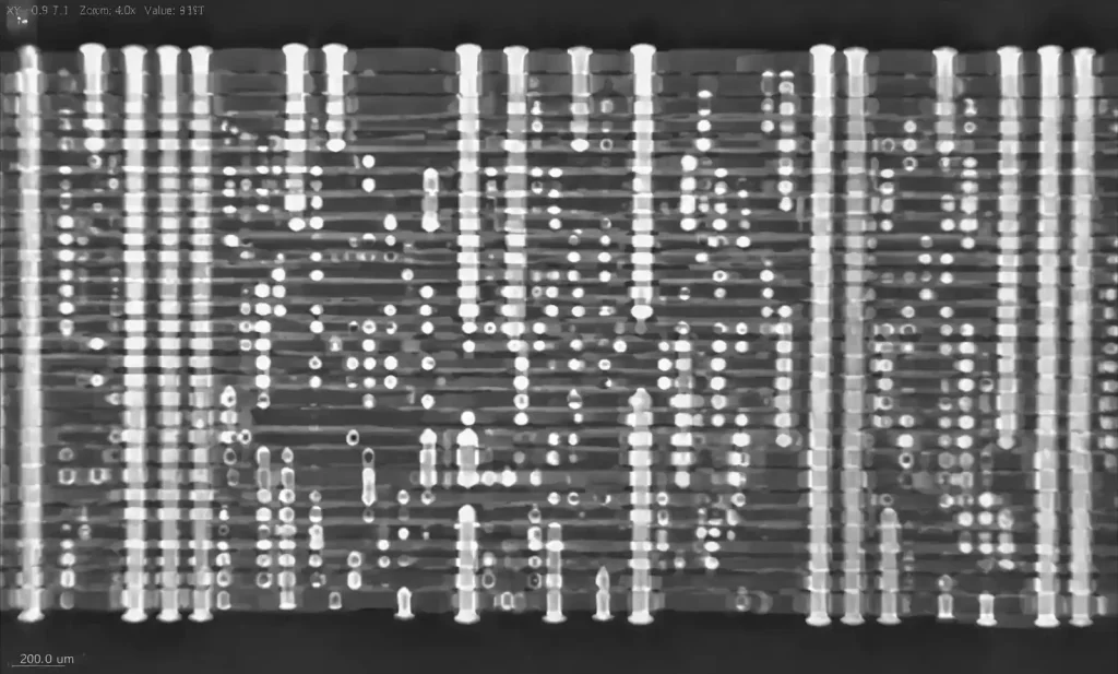
Testing requires specialized equipment beyond standard AOI and flying probe.
X-ray inspection images via structure through 6mm FR-4 to detect voids, cracks, or plating defects invisible from the surface.
Microsectioning involves cutting cross-sections through critical vias, polishing to mirror finish, and examining under 200-400× magnification to measure copper thickness and verify via fill.
Time-domain reflectometry (TDR) verifies impedance-controlled traces maintain ±10% tolerance (50Ω single-ended or 100Ω differential).
Continuity testing with flying probe or bed-of-nails verifies all nets and checks isolation between traces. This takes 2-4 hours per 50-layer board with 5,000+ nets.
These testing requirements add 3-5 days to lead time and $500-1,500 per board to cost.
Cost Factors in 50-Layer Manufacturing
Fifty-layer boards cost 8-12× more than comparable 12-layer boards due to material, processing time, and scrap risk.
A 50-layer board uses 49 copper foil sheets, 48 prepreg layers, and 24 core substrates. Material cost alone: $800-1,200 for a 20cm × 30cm panel before processing.
High-Tg FR-4 (Tg 170-180°C) costs 30-40% more than standard FR-4 but prevents delamination when board temperature exceeds glass transition during reflow.
Sequential lamination requires 3-5 press cycles at 2-4 hours each versus one cycle for standard boards. Total processing: 15-20 working days for 50-layer versus 5-7 days for 12-layer. Rush services (10-12 days) add 60-80% cost premium.
Manufacturing yield runs 60-75% versus 90-95% for standard boards. Common defects: registration errors, via plating voids, inner layer shorts, delamination, warpage. A single defective board costs $3,000-5,000 in wasted materials.
| Specification | 12-Layer Standard | 50-Layer High-Density | Cost Multiple |
|---|---|---|---|
| Material cost | $50-80 per panel | $800-1,200 per panel | 12-16× |
| Processing time | 5-7 days | 15-20 days | 2.5-3× |
| Labor hours | 4-6 hours | 25-35 hours | 5-6× |
| Testing cost | $50-100 per board | $500-1,500 per board | 8-12× |
| Typical yield | 90-95% | 60-75% | Scrap cost 3-4× higher |
| Unit cost (MOQ 10) | $100-200 | $1,800-3,500 | 12-18× |
Applications for 50-Layer PCBs
Ultra-high layer count appears where routing density, signal isolation, or power distribution make lower counts impossible.
5G Telecommunications Infrastructure
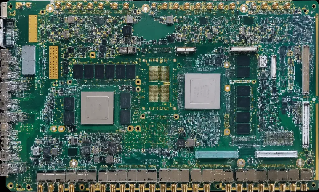
Massive MIMO base stations use 64-256 antenna elements, each requiring RF routing, digital control, and power. The baseband processor board routes hundreds of channels while maintaining controlled impedance for 3.5GHz and 28GHz signals.
A 50-layer stackup provides dedicated RF signal layers with ground isolation, separate power networks for digital/analog/RF sections preventing noise coupling, multiple ground planes at different potentials, and buried microstrip routing without external EMI. Our Special PCB handles these telecommunication applications for major equipment vendors.
Military Radar and Aerospace
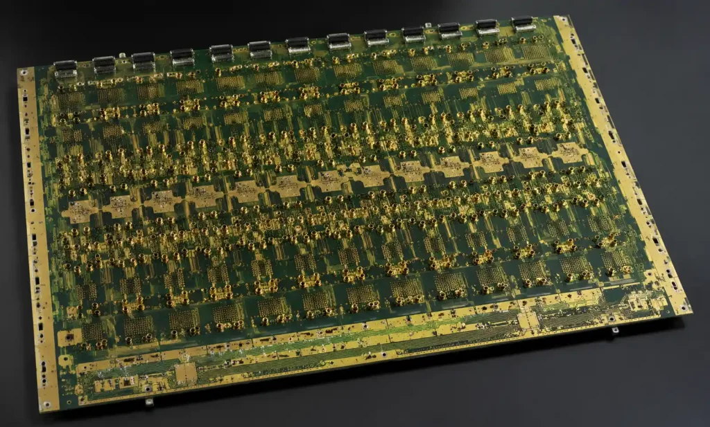
Phased array radar systems use hundreds to thousands of transmit/receive modules. Each needs digital control, RF power, bias voltages, and thermal management routed through the backplane.
Fifty layers enable separate clock networks with matched delays, isolated power planes preventing ground bounce, controlled-impedance RF lines (8-27 GHz), and thermal vias creating heat paths from RF amplifiers to heat sinks.
Defense contractors specify IPC-6012 Class 3 with testing: -55°C to +125°C for 500 cycles, vibration, and salt spray resistance.
AI/ML Compute Systems
GPU accelerator cards route thousands of high-speed differential pairs (PCIe Gen5 at 32 GT/s, NVLink at 100 GB/s per lane) between processor, memory, and interconnect chips.
Fifty-layer stackups solve: signal layer limits forcing wider boards that increase latency, via stubs creating reflections above 20 GHz, power delivery impedance causing voltage droop, and thermal resistance preventing adequate cooling of 400-700W processors.
Design uses 30-35 signal layers for 2,000+ differential pairs, laser microvias eliminating via stubs for clean 20+ GHz transitions, 8-12 power/ground plane pairs providing <1mΩ PDN impedance at 100 MHz, and heavy copper layers (3-6 oz.) spreading heat.
Aerospace Avionics
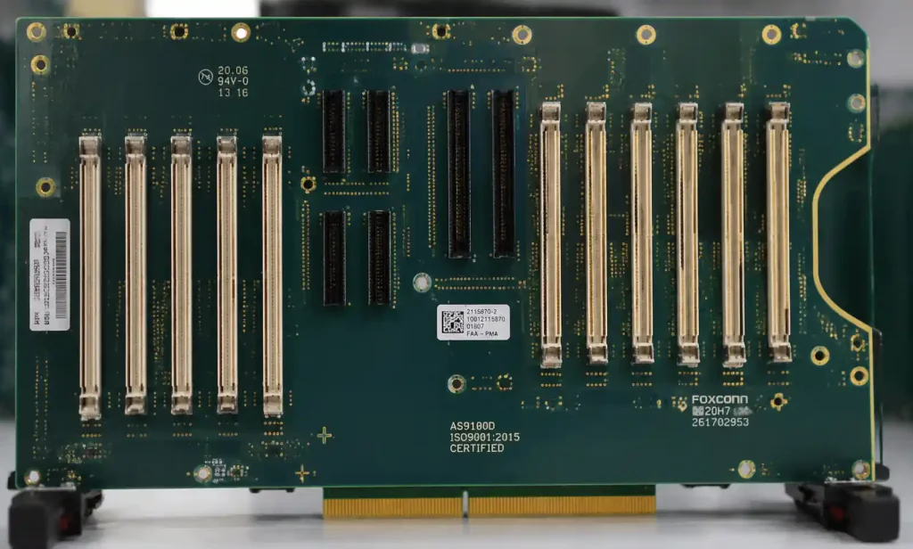
Aircraft avionics backplanes route signals, power, and data buses between flight control, radar, communications, navigation, and displays. A 50-layer backplane consolidates connections reducing aircraft weight 5-15 kg while improving reliability (fewer connectors).
Aerospace PCBs require NASA low-outgassing materials (TML <1.0%, CVCM <0.1%), DO-160 qualification testing, and full traceability for FAA/EASA certification. Andwin Circuits manufactures aviation PCBs meeting AS9100D standards with complete documentation.
Design Considerations for 50-Layer Boards
Work with your fabricator during stackup design to optimize layer arrangement, via structures, and impedance control.
Symmetrical stackup: Fifty-layer boards need mirrored copper and dielectric layers top to bottom to prevent warpage during reflow. Asymmetrical designs warp from unbalanced copper distribution.
Ground and power planes: Reserve every 3rd or 4th layer as continuous ground or power plane, providing return path for adjacent signal layers. Typical: 12 ground planes (layers 3, 7, 11, 15, 19, 23, 27, 31, 35, 39, 43, 47), 12 power planes (5, 9, 13, 17, 21, 25, 29, 33, 37, 41, 45, 49), remaining 26 layers for signal routing.
Thermal management: Six millimeters of FR-4 creates thermal resistance. Components on the surface cool normally, but inner layer circuits need thermal via arrays (50-100 vias on 0.6-0.8mm pitch, 0.3mm diameter, copper-filled) transferring heat to copper planes that spread it laterally—5-10× better conductivity than solid FR-4.
Lead Time and Planning
Plan 15-20 working days for prototypes, 20-25 days for production. Rush services (10-12 days) available with premium pricing.
Order timing: place prototype orders 4-5 weeks before you need assembled boards, schedule production 6-8 weeks before product launch, maintain 2-3 weeks buffer for potential issues.
FAQ
What is the maximum layer count with FR-4 materials?
Current FR-4 technology reliably produces 50-60 layers with proper controls. Beyond 60 layers, thickness exceeds 8-9mm and aspect ratios become unmanageable. Ultra-high counts above 60 require HDI any-layer or embedded component technologies.
What industries use 50-layer PCBs?
Telecommunications (5G), defense and aerospace (radar, avionics), high-performance computing (AI/ML systems), and medical imaging (MRI, CT scanners). Consumer electronics rarely exceed 12-16 layers.
Can you mix standard vias and HDI microvias on 50-layer boards?
Yes. Typical approach: HDI microvias on outer layers (1-8 and 43-50) for fine-pitch components, buried vias in middle section (layers 10-40) for internal routing, through-hole vias only where mechanical strength is needed.
What surface finish works best for 50-layer boards?
ENIG (Electroless Nickel Immersion Gold) provides flat surface for fine-pitch components, 12+ months shelf life, and lead-free reflow compatibility. OSP costs less but has 6-month shelf life and single reflow limitation.
How do you prevent warpage in thick boards?
Use symmetrical stackup, specify high-Tg materials (≥170°C), add stiffener bars for large boards (>300mm), and use fixture support during reflow. Some assemblies require bottom-side preheat.
What IPC standards apply to 50-layer manufacturing?
IPC-6012 covers rigid PCB qualification (Class 2 standard, Class 3 high-reliability). IPC-2221 provides generic design standards. IPC-2226 adds HDI/microvia requirements. Aerospace applications also reference IPC-6018 for microwave/RF boards.
Conclusion
Fifty-layer PCB manufacturing pushes FR-4 technology to practical limits, requiring specialized equipment, experienced engineering, and rigorous quality control. When your design demands routing density, signal integrity, or power distribution beyond standard capabilities, you need a fabricator with proven high-layer-count experience.
The key challenges—registration accuracy, aspect ratio management, sequential lamination, and comprehensive testing—make 50-layer boards 10-15× more expensive than standard multilayer PCBs. But for telecommunications infrastructure, military radar, aerospace avionics, and HPC systems, these costs are necessary when performance requirements exceed lower layer count capabilities.
Andwin Circuits manufactures 50-layer PCBs for telecommunications, aerospace, and defense with ISO 9001, IATF 16949, and AS9100D certifications. Our facility handles boards to 8mm thickness with ±25μm registration accuracy and comprehensive testing including X-ray, TDR, and microsection analysis.