
IC Test Board Design: High-Frequency Probing and Signal Integrity
Semiconductor test engineers report that 30-40% of IC validation failures trace back to test board design issues rather than actual chip defects. When probe contact resistance varies by just 50 milliohms, parametric measurements shift beyond tolerance, and what looks like a failing die is actually a fixture problem.
The difference between a test board and a functional PCB is measurement precision under dynamic load. Your IC test board must deliver stable power, route GHz signals without distortion, isolate hundreds of test channels from crosstalk, and repeat those conditions across 10,000+ probe cycles. This article covers the design rules that separate passing ATE correlation from boards that fail repeatability.
What Makes IC Test Boards Different
IC test boards operate as precision measurement instruments, not signal conduits. The board itself becomes part of the measurement path, where controlled impedance, insertion loss, and contact resistance directly affect parametric accuracy. Test channels must maintain isolation better than -40dB up to the highest test frequency, typically 6-12 GHz for modern high-speed ICs.
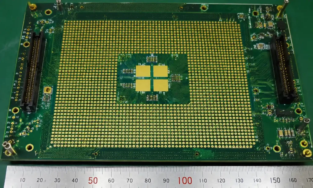
Three factors dominate test board electrical performance: probe contact repeatability, which sets measurement noise floor; channel-to-channel isolation, which determines crosstalk limits; and power delivery impedance, which controls supply droop under switching load. Standard PCB design rules fail here because they optimize for connectivity, not measurement precision.
Probe Pad Design for Reliable Contact
Probe pad geometry controls contact resistance and mechanical wear over thousands of test cycles. Pads require at least 50% larger diameter than the probe tip to accommodate mechanical tolerance and probe touchdown scrub. For spring-loaded probes with 0.5mm tip diameter, specify 0.75-1.0mm pads. Smaller pads increase contact resistance variation and accelerate probe wear.
| Probe Type | Min Pad Diameter | Pad Pitch | Contact Force | Cycle Life |
|---|---|---|---|---|
| Pogo pin (0.5mm tip) | 0.75mm | 1.27mm | 50-100g | 100k+ |
| Cantilever (0.3mm tip) | 0.50mm | 0.8mm | 10-20g | 500k+ |
| Cobra (0.4mm tip) | 0.65mm | 1.0mm | 30-60g | 200k+ |
| Vertical probe (0.6mm tip) | 1.0mm | 1.5mm | 80-150g | 50k+ |
Pad finish affects both contact resistance and longevity. ENIG (Electroless Nickel Immersion Gold) provides the lowest contact resistance, typically under 10 milliohms, and resists oxidation for over 100,000 cycles. Hard gold plating extends cycle life to 500,000+ but requires thicker plating (0.76-1.27μm) and costs 20-30% more. Avoid OSP or HASL finishes on probe pads; both oxidize quickly and push contact resistance above 50 milliohms within 10,000 cycles.
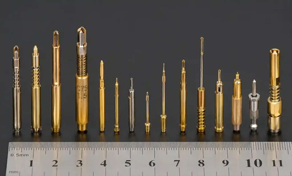
Space pads at minimum 3x probe tip diameter center-to-center to prevent probe shorting. For 0.5mm probes, maintain 1.5mm pitch. Tighter spacing requires custom fixture alignment and increases probe wear from adjacent contact interference.
High-Frequency Signal Routing
Test channels carrying signals above 1 GHz demand transmission line discipline identical to high-speed PCB design. Route every test trace as a controlled impedance line with a continuous reference plane directly beneath it. Match trace impedance to the test system: 50Ω single-ended for most ATE channels, 100Ω differential for high-speed serial links.
Calculate trace width from your PCB stackup and verify with TDR measurement. At 6 GHz, a 10% impedance error generates reflections strong enough to close a 200mV eye. Minimize via count in the signal path as each via adds 0.5-1.5 nH inductance. Use back-drilled stubs when vias are unavoidable. Match all signal paths to within 5mm for multi-site parallel test to keep timing correlation tight.
Crosstalk Prevention Between Test Channels
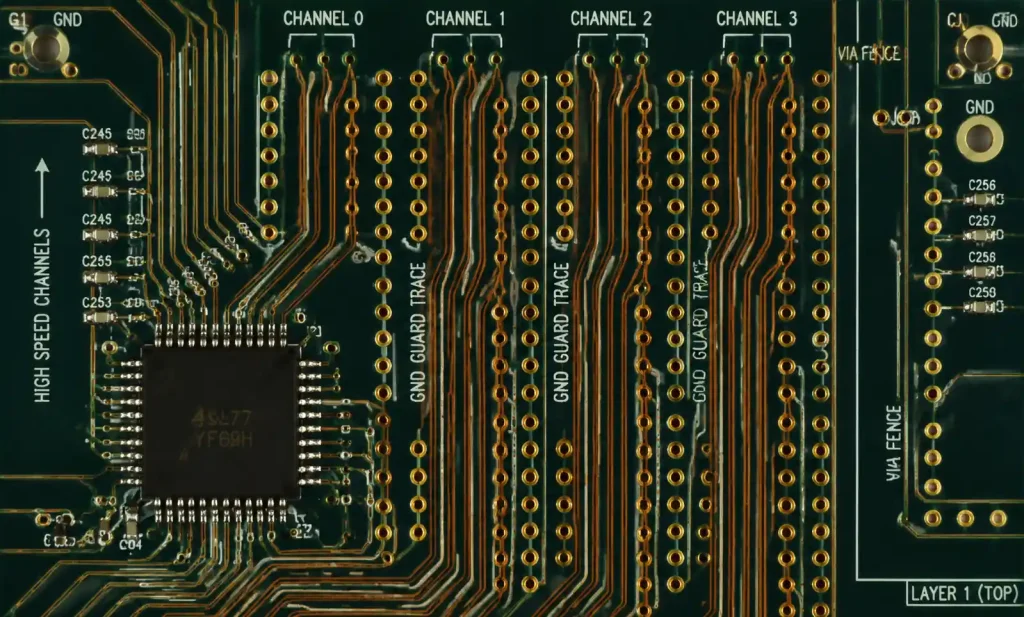
IC test boards pack hundreds of high-frequency channels into dense arrays where adjacent traces couple through electromagnetic fields. Crosstalk above -40dB corrupts neighboring channels and creates false failures. Spacing, shielding, and reference plane integrity control coupling.
| Trace Spacing (W) | Crosstalk Level | Use Case |
|---|---|---|
| 1x trace width | -25dB (5.6%) | Low-speed I/O, < 100 MHz |
| 3x trace width | -40dB (1%) | General digital, < 1 GHz |
| 5x trace width | -50dB (0.3%) | RF, high-speed SerDes, > 3 GHz |
| Grounded guard trace | -55dB (0.18%) | Precision analog test |
Increase spacing to 3x trace width minimum for channels above 500 MHz. Where density demands tighter routing, insert grounded guard traces between sensitive channels with stitching vias every 50-100 mils. Never route traces over plane splits; gaps force return current detours that radiate EMI. Run parallel traces on adjacent layers at 90-degree rotation to cut coupling by 15-20dB.
Power Delivery Network Design
IC test requires stable power with less than 10mV of supply droop during switching events. The power delivery network (PDN) must provide low impedance from DC through the highest switching frequency, typically 100 MHz to 1 GHz for modern logic.
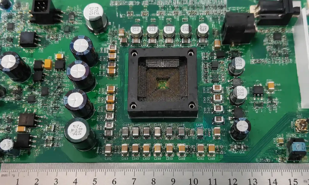
Place bulk capacitors (10-100μF) within 10mm of the DUT, mid-frequency capacitors (1-10μF) within 3mm of power pins, and high-frequency capacitors (0.01-0.1μF) directly adjacent to each power pin. Use Kelvin connections for power delivery to separate the supply path from the voltage sense path, cutting supply droop by 50-100mV on high-current rails.
Connect decoupling capacitors with the shortest via path. A 0.1μF capacitor with 10nH via inductance stops decoupling above 50 MHz. Use via-in-pad construction to minimize inductance. Pour solid ground and power planes across the board to avoid return current barriers.
Kelvin Sensing for Accurate Measurement
Parametric test accuracy depends on measuring voltage exactly at the DUT pins, not at the connector where IR drop adds measurement error. Kelvin sensing routes separate force and sense lines to each critical pin. The force lines carry test current through low-impedance traces. The sense lines connect to high-impedance measurement inputs and carry negligible current, so IR drop is near zero.
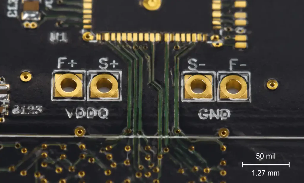
Route sense traces separately from force traces with 3x trace width spacing to prevent coupling. Keep sense trace length below 50mm to minimize parasitic capacitance. Kelvin probe pads require four contacts per power pin: force+, force-, sense+, and sense-. This cuts measurement error from 50-100mV down to under 1mV on low-voltage supplies.
Test Fixture Integration
The test board mounts into a mechanical fixture that aligns probes to pads and interfaces to ATE hardware. Probe length determines parasitic inductance: standard spring probes are 10-15mm with 8-12 nH inductance; custom short-stack probes reach 5-7mm with 4-6 nH but cost 3-5x more. Target probe self-resonance at least 3x above test frequency.
Maintain probe contact force within ±20% across the array. Force variation creates contact resistance variation that appears as measurement noise. Design adequate thermal management for high-power ICs; power above 5W requires forced air or liquid cooling.
Andwin Circuits manufactures precision test boards up to 50 layers with tight impedance control and microvias for dense probe pad arrays. Our HDI PCB capabilities support probe pitches down to 0.4mm, with fast delivery in 7 days.
FAQs
What probe pad finish provides the lowest contact resistance?
ENIG (Electroless Nickel Immersion Gold) delivers the lowest contact resistance, typically 5-10 milliohms, and maintains stable performance for over 100,000 cycles. Hard gold plating extends cycle life to 500,000+ but requires 0.76-1.27μm thickness and adds 20-30% cost compared to standard ENIG.
How tight should impedance tolerance be for GHz test signals?
Target ±5-7% impedance tolerance for test channels above 3 GHz. Looser tolerance generates reflections that corrupt eye diagrams. Work with your PCB manufacturer to verify impedance through TDR testing.
Why use Kelvin sensing instead of two-wire measurement?
Kelvin sensing eliminates IR drop by routing separate force and sense lines. This cuts measurement error from 50-100mV to under 1mV on low-voltage supplies. For high-current rails above 1A, Kelvin connections are mandatory.
What causes crosstalk between test channels?
Crosstalk results from electromagnetic coupling between adjacent traces. Spacing traces at 3x trace width reduces coupling to -40dB, adequate for most digital channels. RF and high-speed serial channels may require 5x spacing or grounded guard traces.
How do I calculate required via count for power planes?
Target one via per 100-200mA of peak switching current, placed near decoupling capacitors. For a 5A power rail, use 25-50 vias distributed across the DUT footprint with 0.3-0.4mm diameter.
Conclusion
IC test board design demands transmission line discipline, precision measurement technique, and mechanical repeatability that standard PCB design rules do not address. Probe pad geometry, four-wire Kelvin sensing, controlled crosstalk, and clean power delivery separate test boards that correlate with ATE from those that inject measurement noise and create false failures.
If you need high-performance IC test boards for semiconductor validation, Andwin Circuits offers advanced manufacturing capabilities up to 50 layers with controlled impedance, precision probe pad arrays, and tight dimensional tolerance. Our ISO 9001 certified facility delivers prototype test boards in 7 days with full electrical verification, supporting high-speed digital, RF, and mixed-signal IC test applications.
Contact us today for custom IC test board manufacturing with factory-direct pricing and engineering support for your ATE integration.