Alumina vs Aluminum Nitride Ceramic PCB: Which Substrate Material is Right for Your Project?
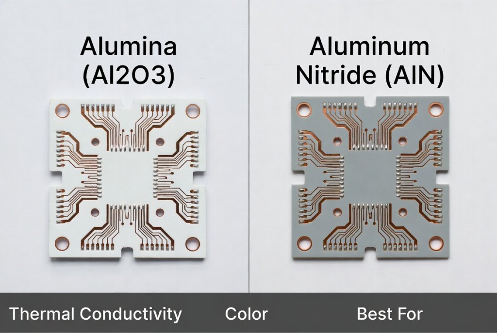
Figure 1: Ceramic PCB substrate material comparison between Alumina (Al₂O₃) and Aluminum Nitride (AlN)
Introduction
Selecting the optimal substrate material for your high-power electronics project can mean the difference between product success and catastrophic failure. As power densities continue to rise across industries—from electric vehicles to 5G telecommunications—the demand for advanced thermal management solutions has never been more critical. This is where ceramic PCB technology emerges as a game-changing solution, offering thermal performance that traditional FR4 boards simply cannot match.
Analysis indicates that the global ceramic PCB market, valued at $1.73 billion in 2026, is projected to reach $3.49 billion by 2035, driven by a 7.5% compound annual growth rate. This explosive growth reflects the critical role ceramic substrates play in modern electronics manufacturing. Among the various ceramic materials available, Alumina (Al₂O₃) and Aluminum Nitride (AlN) stand out as the two most widely adopted options, each offering distinct advantages for specific applications.
Whether you’re designing high-power LED modules, EV inverters, or RF amplifiers, understanding the nuanced differences between these two substrate materials is essential for making an informed decision. This comprehensive guide will walk you through everything you need to know about selecting the right ceramic substrate for your project requirements.
Quick Answer
Alumina (Al₂O₃) ceramic PCBs offer cost-effective thermal management with 24-30 W/m·K conductivity, ideal for medium-power applications where budget constraints matter. Aluminum Nitride (AlN) delivers superior thermal performance at 170-230 W/m·K, making it the preferred choice for high-power density applications where heat dissipation is mission-critical. Your selection should be based on power requirements, thermal budget, and cost considerations.
Table of Contents
- Understanding the Thermal Management Challenge
- Material Deep Dive: Alumina (Al₂O₃) Ceramic PCB
- Material Deep Dive: Aluminum Nitride (AlN) Ceramic PCB
- Head-to-Head Comparison: Technical Specifications
- Manufacturing Technologies for Ceramic PCBs
- Application-Specific Selection Guide
- Cost Analysis and ROI Considerations
- How to Select the Right Ceramic Substrate
- Industry Applications and Use Cases
- Frequently Asked Questions
- Conclusion: Making the Right Choice
1. Understanding the Thermal Management Challenge
The Heat Dissipation Problem in Modern Electronics
Modern electronic devices are pushing the boundaries of power density like never before. Data reveals that a typical high-power LED array can generate heat fluxes exceeding 100 W/cm², while EV power inverters operate at currents surpassing 200A with temperatures soaring past 150°C. Traditional FR4 printed circuit boards, with thermal conductivity of merely 0.25-0.4 W/m·K, simply cannot handle these thermal loads effectively.
The consequences of inadequate thermal management are severe:
- Component degradation: Every 10°C increase in junction temperature can reduce semiconductor lifespan by 50%
- Performance throttling: Thermal protection circuits may limit device output to prevent damage
- System failures: Solder joint fatigue and delamination under thermal cycling
- Warranty costs: Field failures can cost manufacturers 10x more than premium substrate investments
Why Ceramic PCBs Are the Solution
Ceramic PCB technology addresses these challenges through materials that combine exceptional thermal conductivity with excellent electrical insulation. Unlike organic substrates, ceramics can withstand operating temperatures up to 800°C while providing thermal conductivity 60-100x higher than FR4.
Key Insight: Research from the Journal of Electronic Materials demonstrates that switching from FR4 to Alumina ceramic PCB can reduce junction temperatures by 30-40°C in power LED applications, directly extending component lifetime from 10,000 hours to over 50,000 hours.
2. Material Deep Dive: Alumina (Al₂O₃) Ceramic PCB
What is Alumina Ceramic?
Alumina (Aluminum Oxide, Al₂O₃) is the most widely used ceramic substrate material in the electronics industry. Available primarily in 96% and 99.6% purity grades, Alumina has established itself as the workhorse of ceramic PCB manufacturing due to its excellent balance of performance, reliability, and cost-effectiveness.
Key Properties of Alumina Ceramic PCB
Thermal Performance:
- Thermal conductivity: 24-30 W/m·K (96% grade), 28-35 W/m·K (99.6% grade)
- Maximum operating temperature: 800°C+
- Coefficient of thermal expansion: 6.5-7.5 ppm/°C
Electrical Characteristics:
- Dielectric constant: 9.0-10.0 at 1MHz
- Dielectric strength: 15+ kV/mm
- Volume resistivity: 10¹⁴ Ω·cm
Mechanical Properties:
- Flexural strength: 350-400 MPa
- Hardness: 1600 HV (excellent wear resistance)
- Density: 3.75-3.95 g/cm³
Advantages of Alumina Ceramic PCB
- Cost-Effectiveness: Alumina offers the most affordable entry point into ceramic PCB technology, typically 3-5x less expensive than Aluminum Nitride
- Proven Reliability: Decades of field data support Alumina’s long-term performance in demanding applications
- Manufacturing Maturity: Well-established supply chains and processing techniques ensure consistent quality and availability
- Excellent Electrical Insulation: High dielectric strength makes Alumina ideal for high-voltage applications
- Mechanical Durability: Superior hardness and wear resistance compared to other ceramic options
Limitations to Consider
- Thermal Performance Ceiling: While significantly better than FR4, Alumina’s thermal conductivity may be insufficient for extremely high-power density applications
- CTE Mismatch: Higher thermal expansion coefficient compared to silicon chips can create mechanical stress during thermal cycling
- RF Performance: Higher dielectric constant and loss tangent limit high-frequency applications
Typical Applications
- Medium-power LED modules and COB (Chip-on-Board) applications
- Industrial control circuits and power supplies
- Automotive sensor modules and ignition systems
- Medical device electronics
- General-purpose hybrid integrated circuits
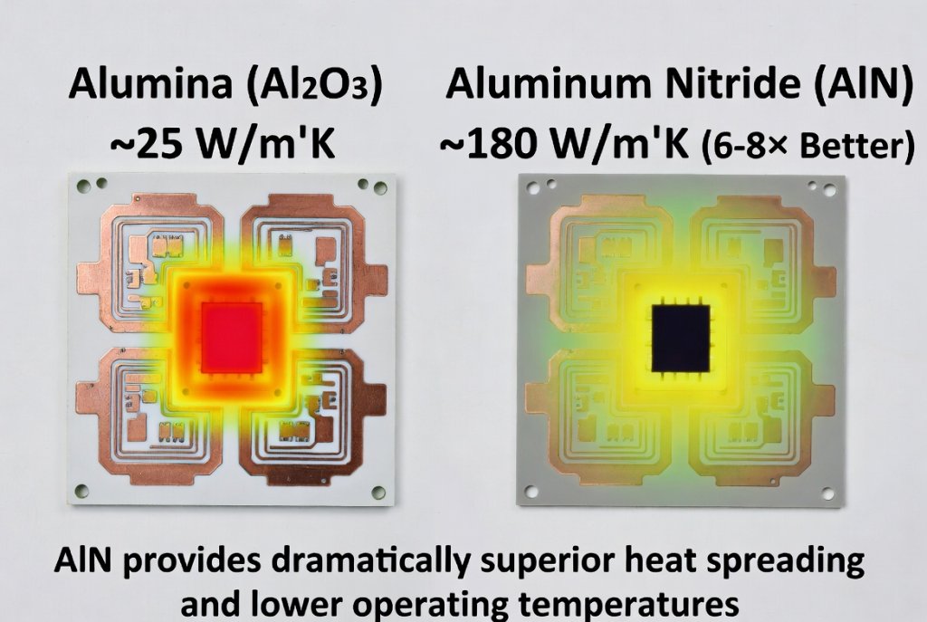
Figure 2: Thermal conductivity comparison showing AlN’s 6-8x superior heat dissipation capability
3. Material Deep Dive: Aluminum Nitride (AlN) Ceramic PCB
What is Aluminum Nitride Ceramic?
Aluminum Nitride (AlN) represents the premium tier of ceramic substrate materials, offering thermal conductivity that rivals some metals while maintaining excellent electrical insulation. With thermal performance 6-8x superior to Alumina, AlN has become the substrate of choice for applications where heat dissipation is the primary design constraint.
Key Properties of Aluminum Nitride Ceramic PCB
Thermal Performance:
- Thermal conductivity: 170-230 W/m·K (theoretical maximum: 320 W/m·K)
- Maximum operating temperature: 850°C+
- Coefficient of thermal expansion: 4.5-5.5 ppm/°C (closely matching silicon)
Electrical Characteristics:
- Dielectric constant: 8.5-8.9 at 1MHz
- Dielectric loss: 2.0 × 10⁻³ (excellent for RF applications)
- Volume resistivity: 10¹³-10¹⁴ Ω·cm
Mechanical Properties:
- Flexural strength: 350 MPa
- Fracture toughness: 4.0 MPa·m¹/²
- Density: 3.26 g/cm³
Advantages of Aluminum Nitride Ceramic PCB
- Unmatched Thermal Conductivity: At 170-230 W/m·K, AlN approaches the thermal performance of beryllium oxide (BeO) without the toxicity concerns
- CTE Matching with Silicon: The thermal expansion coefficient of 4.5 ppm/°C closely matches silicon (2.6-3.5 ppm/°C), minimizing thermal stress on bonded components
- Superior RF Performance: Lower dielectric constant and loss tangent enable high-frequency applications up to millimeter-wave frequencies
- Thermal Shock Resistance: Excellent resistance to rapid temperature cycling without cracking or delamination
- Environmental Safety: Non-toxic alternative to beryllium oxide, complying with RoHS and environmental regulations
Limitations to Consider
- Higher Cost: AlN substrates typically cost 3-5x more than equivalent Alumina substrates
- Processing Sensitivity: Requires careful handling during manufacturing to prevent surface oxidation
- Moisture Sensitivity: Can be susceptible to surface hydrolysis under high-temperature, high-humidity conditions
- Mechanical Strength: Slightly lower flexural strength compared to Alumina
Typical Applications
- High-power LED lighting (automotive headlights, industrial grow lights)
- EV traction inverters and power modules
- RF amplifiers and 5G base station equipment
- Laser diode carriers and optical communications
- Wide bandgap semiconductor packaging (SiC, GaN devices)
- Aerospace and defense electronics
4. Head-to-Head Comparison: Technical Specifications
The following comprehensive comparison table provides a side-by-side analysis of Alumina and Aluminum Nitride ceramic PCB substrates across all critical performance parameters:
| Property | Alumina (Al₂O₃) 96% | Alumina (Al₂O₃) 99.6% | Aluminum Nitride (AlN) | Design Impact |
|---|---|---|---|---|
| Thermal Conductivity (W/m·K) | 24-28 | 28-35 | 170-230 | AlN provides 6-8x better heat dissipation |
| CTE (ppm/°C) | 6.5-7.5 | 7.0-7.4 | 4.5-5.5 | AlN matches silicon chips better |
| Dielectric Constant (1MHz) | 9.0-9.8 | 9.5-9.9 | 8.5-8.9 | AlN preferred for high-frequency RF |
| Dielectric Loss (×10⁻³) | 3.0 | 2.5-3.0 | 2.0 | Lower loss means better signal integrity |
| Flexural Strength (MPa) | 350 | 400 | 350 | High-purity Alumina strongest |
| Hardness (HV) | 1600 | 1800 | 1150 | Alumina offers superior wear resistance |
| Max Operating Temp (°C) | 800+ | 1000+ | 850+ | All ceramics excel at high temperatures |
| Relative Cost | Low | Low-Medium | High | Alumina most cost-effective option |
Key Takeaways from the Comparison
Critical Insight: When power density exceeds 50 W/cm², Aluminum Nitride becomes the economically rational choice despite higher upfront costs. The improved thermal performance directly translates to extended component lifetime, reduced warranty claims, and improved system reliability.
The data clearly shows that material selection involves trade-offs between thermal performance, mechanical properties, and cost. While AlN dominates in thermal conductivity and RF performance, Alumina offers superior mechanical hardness and cost-effectiveness for less demanding applications.
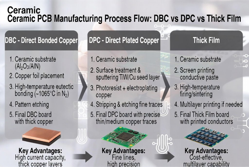
Figure 3: Ceramic PCB manufacturing process flow showing DPC, DBC, and Thick Film technologies
5. Manufacturing Technologies for Ceramic PCBs
Understanding the manufacturing processes behind ceramic PCBs is essential for making informed design decisions. Three primary technologies dominate the industry: Direct Plated Copper (DPC), Direct Bonded Copper (DBC), and Thick Film.
Direct Plated Copper (DPC) Technology
DPC is the most advanced manufacturing method, offering the finest trace resolution and best surface finish for high-frequency applications.
Process Overview:
- Ceramic substrate preparation and cleaning
- Laser etching for circuit pattern definition
- Sputter deposition of seed layer (Ti/W)
- Photoresist coating and patterning
- Electroplating of copper traces
- Photoresist removal and final finishing
Advantages:
- Minimum trace width/spacing: 25/25 μm
- Excellent surface smoothness for RF applications
- Precise copper thickness control
- Suitable for complex, high-density designs
Best Applications:
- High-frequency RF and microwave circuits
- Precision sensor modules
- Semiconductor packaging substrates
- Fine-pitch LED arrays
Direct Bonded Copper (DBC) Technology
DBC bonding creates an exceptionally strong metallurgical bond between copper and ceramic, ideal for high-current power applications.
Process Overview:
- Copper foil oxidation treatment
- Ceramic substrate preparation
- Eutectic bonding at 1065-1083°C
- Pattern etching using photolithography
- Final finishing and testing
Advantages:
- Copper thickness: up to 300-800 μm
- Superior copper adhesion strength
- Excellent current-carrying capability
- Cost-effective for high-volume production
Best Applications:
- Power modules and IGBT substrates
- High-current LED drivers
- EV inverter boards
- Industrial heating elements
Thick Film Technology
The traditional and most economical method, thick film printing uses conductive pastes to create circuit patterns.
Process Overview:
- Screen printing of conductive paste (Ag, Au, Cu)
- Drying at 150°C
- Firing at 850-900°C
- Repeat for multilayer structures
- Optional resistor printing
Advantages:
- Lowest manufacturing cost
- Simple, high-volume process
- Integrated resistor capability
- No photolithography required
Best Applications:
- Cost-sensitive LED substrates
- General-purpose power electronics
- Heater circuits
- Sensor housings
6. Application-Specific Selection Guide
When to Choose Alumina (Al₂O₃) Ceramic PCB
Select Alumina when your application meets the following criteria:
✅ Cost optimization is a primary concern
- Budget-constrained projects requiring ceramic benefits
- High-volume consumer electronics
- Cost-sensitive industrial applications
✅ Thermal requirements are moderate
- Power density below 50 W/cm²
- Operating temperatures below 150°C junction temperature
- Adequate heat sinking available
✅ High electrical insulation is critical
- High-voltage isolation applications
- Power supply and converter circuits
- Medical equipment requiring patient safety isolation
✅ Mechanical durability is important
- Applications with vibration or shock
- Wear-resistant surfaces required
- Rugged industrial environments
✅ Standard thick-film hybrid circuits
- Legacy product designs
- Cost-sensitive LED modules
- General-purpose power electronics
When to Choose Aluminum Nitride (AlN) Ceramic PCB
Select Aluminum Nitride when your application demands:
✅ Maximum thermal performance
- Power density exceeding 100 W/cm²
- Limited heat sinking or space constraints
- High-power LED arrays and laser diodes
✅ Wide bandgap semiconductor packaging
- SiC (Silicon Carbide) devices
- GaN (Gallium Nitride) power amplifiers
- High-frequency RF power modules
✅ High-frequency RF/microwave applications
- 5G base station equipment
- Radar and communication systems
- Millimeter-wave circuits
✅ Severe thermal cycling conditions
- Automotive under-hood applications
- Aerospace and defense systems
- Industrial equipment with frequent on/off cycles
✅ High-reliability systems justify premium cost
- Mission-critical aerospace electronics
- Medical implant devices
- Telecommunications infrastructure
7. Cost Analysis and ROI Considerations
Understanding the Total Cost of Ownership
When evaluating ceramic PCB substrates, it’s essential to look beyond the initial material cost and consider the total cost of ownership (TCO) over the product lifecycle.
Initial Material Cost Comparison:
| Cost Factor | Alumina (Al₂O₃) | Aluminum Nitride (AlN) |
|---|---|---|
| Raw Material Cost | $ (Lowest) | $$$ (3-5x higher) |
| Processing Cost | $ (Mature processes) | $$ (Specialized handling) |
| Yield Impact | Standard | May improve with better thermal performance |
| System-Level Savings | Moderate | Significant (reduced heat sinks, smaller size) |
ROI Calculation Framework
Consider this real-world scenario for a high-power LED lighting application:
Scenario: 100W LED module operating 12 hours/day
| Factor | Alumina PCB | AlN PCB |
|---|---|---|
| Substrate Cost | $15 | $60 |
| Junction Temperature | 95°C | 65°C |
| Expected LED Lifetime | 25,000 hours | 60,000 hours |
| Replacement Cycle | 5.7 years | 13.7 years |
| Total 10-Year Cost | $45 (2 replacements) | $60 (no replacement) |
Analysis: Despite the 4x higher initial cost, the AlN substrate actually delivers lower total cost of ownership while providing superior reliability. This calculation doesn’t include additional savings from reduced warranty claims and improved customer satisfaction.
Expert Recommendation: For applications with power density below 30 W/cm², Alumina typically provides the optimal cost-performance balance. Above 50 W/cm², the performance advantages of AlN generally justify the premium cost.
8. How to Select the Right Ceramic Substrate
Step-by-Step Selection Process
Follow this systematic approach to determine the optimal ceramic substrate for your project:
Step 1: Define Thermal Requirements
- Calculate maximum power dissipation (W)
- Determine allowable junction temperature (°C)
- Assess available heat sinking and cooling options
- Calculate required thermal resistance (°C/W)
Step 2: Evaluate Electrical Requirements
- Operating voltage and isolation requirements
- Signal frequency and RF performance needs
- Dielectric constant and loss tangent specifications
- Current-carrying capacity requirements
Step 3: Assess Mechanical Constraints
- Physical size and thickness requirements
- Vibration and shock environment
- Thermal cycling profile (number of cycles, temperature range)
- Assembly method (wire bonding, solder attach, etc.)
Step 4: Determine Budget Parameters
- Target unit cost at volume
- Total cost of ownership considerations
- Warranty and reliability requirements
- Time-to-market constraints
Step 5: Match Requirements to Material Properties
Use this decision matrix:
Power Density < 30 W/cm² + Cost Sensitive → Alumina
Power Density 30-50 W/cm² + Balanced → Either (detailed analysis needed)
Power Density > 50 W/cm² + Performance Critical → Aluminum Nitride
High Frequency RF (>5 GHz) → Aluminum Nitride
Severe Thermal Cycling (>5000 cycles) → Consider Silicon Nitride
Consulting with Manufacturing Partners
Working with an experienced ceramic PCB manufacturer can provide valuable guidance during the selection process. Look for partners who offer:
- Material selection consultation and thermal modeling
- Prototype and sample evaluation programs
- Design for manufacturability (DFM) feedback
- Application-specific testing and validation
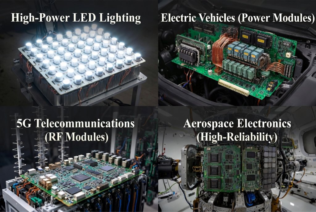
Figure 4: Ceramic PCB applications across high-power LED lighting, electric vehicles, 5G telecommunications, and aerospace electronics
9. Industry Applications and Use Cases
High-Power LED Lighting
The LED lighting industry has been a major adopter of ceramic PCB technology, driven by the need to manage heat from increasingly powerful LED arrays.
Application Requirements:
- Thermal conductivity: 24-230 W/m·K depending on power level
- Electrical isolation for safety compliance
- Long-term reliability (50,000+ hour lifetime)
Material Selection Guidance:
- 3W-10W LED modules: Alumina (Al₂O₃) provides adequate thermal management at optimal cost
- 50W-200W automotive headlights: Aluminum Nitride (AlN) essential for heat dissipation
- Industrial grow lights (>500W): AlN with DBC technology for maximum thermal performance
Case Study: A leading automotive lighting manufacturer switched from Alumina to AlN substrates for their LED headlight modules. The result: 35°C reduction in junction temperature, extended LED lifetime from 15,000 to 45,000 hours, and elimination of thermal-related warranty claims.
Electric Vehicle Power Electronics
EV inverters, onboard chargers, and DC-DC converters represent some of the most demanding applications for ceramic PCB substrates.
Application Requirements:
- Power density: 100-300 W/cm²
- Operating temperature: -40°C to 150°C ambient
- Thermal cycling: Thousands of cycles over vehicle lifetime
- Reliability: 15+ year vehicle lifetime
Material Selection Guidance:
- Traction inverters: AlN substrates with DBC copper for IGBT/SiC modules
- Onboard chargers: Alumina DBC for cost-effective power handling
- Battery management systems: Alumina for sensor and control electronics
5G Telecommunications Infrastructure
5G base stations and small cells require ceramic substrates that can handle high-frequency RF signals while managing heat from power amplifiers.
Application Requirements:
- Frequency range: 3.5 GHz to 28 GHz (mmWave)
- Low dielectric loss for signal integrity
- Thermal management for power amplifiers (50-200W)
Material Selection Guidance:
- Power amplifiers: AlN for thermal performance and low dielectric loss
- Antenna arrays: AlN for RF performance at mmWave frequencies
- Baseband processing: Alumina for cost-effective digital circuits
Aerospace and Defense Electronics
Aerospace applications demand the highest reliability under extreme environmental conditions.
Application Requirements:
- Operating temperature: -55°C to 125°C (often wider)
- Vibration and shock resistance
- Radiation tolerance for space applications
- Long-term reliability (20+ years for satellites)
Material Selection Guidance:
- Satellite power systems: AlN for thermal performance in vacuum
- Avionics: Alumina for cost-effective, proven reliability
- Radar systems: AlN for high-power RF amplifiers
Medical Equipment
Medical devices require ceramic substrates that combine reliability with biocompatibility and electrical safety.
Application Requirements:
- High electrical isolation for patient safety
- Long-term reliability (10-20 year device lifetime)
- Biocompatibility for implantable devices
- Precision and stability for diagnostic equipment
Material Selection Guidance:
- Imaging equipment (MRI, CT): AlN for RF performance and thermal management
- Implantable devices: Alumina for proven biocompatibility
- Surgical equipment: Alumina for cost-effective, reliable performance
10. Frequently Asked Questions
What is the main difference between Alumina and Aluminum Nitride ceramic PCBs?
The primary difference lies in thermal conductivity. Alumina (Al₂O₃) offers 24-30 W/m·K thermal conductivity, while Aluminum Nitride (AlN) delivers 170-230 W/m·K—approximately 6-8x better heat dissipation. This makes AlN the preferred choice for high-power density applications where thermal management is critical, while Alumina provides a cost-effective solution for moderate power requirements.
How much more expensive is Aluminum Nitride compared to Alumina?
Aluminum Nitride substrates typically cost 3-5 times more than equivalent Alumina substrates. However, the total cost of ownership analysis often reveals that AlN’s superior thermal performance can actually reduce overall system costs by:
- Eliminating or reducing external heat sinks
- Extending component lifetime (reducing replacement costs)
- Improving system reliability (reducing warranty claims)
- Enabling smaller, lighter product designs
Can I use Alumina for high-power LED applications?
Yes, Alumina is suitable for low to medium-power LED applications (typically up to 50W). For higher power levels or applications with limited heat sinking, Aluminum Nitride becomes the better choice. The decision depends on:
- LED power density (W/cm²)
- Available thermal management (heat sinks, airflow)
- Target LED lifetime and reliability requirements
- Cost constraints
What manufacturing technologies are available for ceramic PCBs?
Three primary manufacturing technologies are used for ceramic PCBs:
- DPC (Direct Plated Copper): Offers finest trace resolution (25/25 μm), best for RF and precision applications
- DBC (Direct Bonded Copper): Provides thick copper layers (up to 800 μm), ideal for high-current power modules
- Thick Film: Most economical method using screen-printed conductive pastes, suitable for cost-sensitive applications
Is Aluminum Nitride safe to handle?
Yes, Aluminum Nitride is non-toxic and safe to handle, unlike beryllium oxide (BeO) which requires special safety precautions. AlN has become the preferred alternative to BeO for high-thermal-conductivity applications, offering similar thermal performance without the health and environmental concerns.
How do I determine which ceramic substrate is right for my project?
Follow this decision framework:
- Calculate your power density (W/cm²)
- Determine your thermal budget and heat sinking capability
- Assess your electrical requirements (voltage, frequency)
- Consider your mechanical environment (vibration, thermal cycling)
- Define your cost constraints and reliability targets
General rule: Power density below 30 W/cm² → Alumina; above 50 W/cm² → Aluminum Nitride
What is the typical lead time for ceramic PCB manufacturing?
Lead times vary based on technology and complexity:
- Standard Alumina (Thick Film): 2-3 weeks
- Alumina DPC/DBC: 3-4 weeks
- Aluminum Nitride DPC/DBC: 4-6 weeks
- Custom designs: 8-12 weeks including prototyping
For urgent projects, look for manufacturers offering Custom service with 7-day rapid delivery to accelerate your time-to-market.
Can ceramic PCBs be used for flexible circuits?
Traditional ceramic PCBs are rigid substrates. However, flexible ceramic circuits can be created using:
- Thin ceramic substrates (0.1-0.25 mm) with limited flexibility
- Ceramic-filled polymer composites for semi-flexible applications
- Hybrid constructions combining ceramic islands with flexible interconnects
For truly flexible applications, polyimide-based flexible circuits remain the standard solution.
11. Conclusion: Making the Right Choice
Summary of Key Findings
The choice between Alumina (Al₂O₃) and Aluminum Nitride (AlN) ceramic PCB substrates ultimately depends on your specific application requirements, thermal budget, and cost constraints.
Choose Alumina when:
- Cost optimization is a primary concern
- Power density is below 50 W/cm²
- High electrical insulation is required
- Mechanical durability is important
- You’re seeking a proven, reliable solution with mature supply chains
Choose Aluminum Nitride when:
- Maximum thermal performance is required (power density >100 W/cm²)
- You’re packaging wide bandgap semiconductors (SiC, GaN)
- High-frequency RF performance is critical
- Severe thermal cycling conditions are expected
- System reliability justifies the premium investment


