Assembling printed circuit boards
1.The process of assembling a circuit board
Assembling printed circuit boards (PCBs) is a vital part of the electronics manufacturing process. First, the design stage is the starting point of the entire process. At this stage, engineers use professional design software to create circuit diagrams and layouts. After the design is completed, the generated Gerber files will be sent to the manufacturer for the production of PCB boards. Next, the manufacturer will perform processes such as drawing, etching and drilling according to these files to finally form a bare board.
Next, enter the procurement and preparation stage of components. The selection and procurement of components need to be strictly in accordance with the design requirements to ensure the functionality and performance of the circuit. After the components arrive, they need to be quality checked and sorted so that the subsequent assembly work can proceed smoothly. At this time, the correctness and integrity of the components are crucial, because any error may cause the failure of the entire circuit.
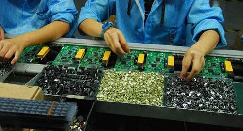
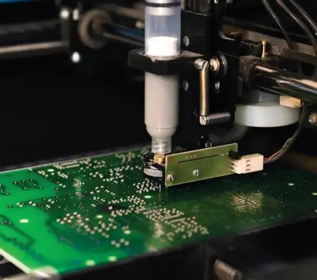
Then, enter the welding stage, which is one of the core steps of assembling PCB boards. First, surface mount technology (SMT) welding is carried out. The surface mount components (SMD) are accurately placed at the designated position of the PCB board through an automatic placement machine. Subsequently, the PCB board will pass through a reflow soldering oven, and the solder paste will melt at high temperature to form a firm solder joint. For some components that need manual soldering, such as high-power components or components with special packages, manual soldering is required.
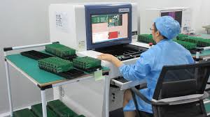
After soldering is completed, electrical testing and functional testing are key steps to ensure the quality of PCB boards. Through automatic optical inspection (AOI) and X-ray inspection, defects that may occur during soldering, such as cold soldering, short circuits and open circuits, can be found. Subsequently, functional testing is performed to ensure that the circuit board can work properly in actual applications. This step not only verifies the correctness of the circuit design, but also promptly detects and repairs potential problems.
Finally, cleaning and protection treatment are performed. The solder paste and flux used in the soldering process may remain on the PCB board, affecting the performance and reliability of the circuit. Therefore, special cleaning equipment and solvents are required to thoroughly remove these residues. After cleaning, a protective layer such as three-proof paint can be applied as needed to improve the environmental resistance and service life of the PCB board.
In summary, assembling PCB boards is a complex and delicate process, and every step is crucial. From design, component procurement, soldering to testing and protection, every link requires strict control and precise operation to ensure the quality and reliability of the final product. Through the detailed analysis of these key steps, we can better understand and master the entire process of PCB board assembly, laying a solid foundation for the manufacture of high-quality electronic products.
GET PCB MANUFACTURING AND ASSEMBLY QUOTE NOW!
2.How to assemble electronic components
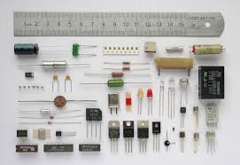
Assembling electronic components is a job that requires meticulousness and patience, and a comprehensive guide from basic to advanced will help you master this skill. First, it is crucial to understand the basic electronic components. Common electronic components include resistors, capacitors, diodes, and transistors, etc. Each component has its specific function and purpose, so before assembly, it is necessary to be familiar with their characteristics and identification methods.
Next, prepare the required tools and materials. Commonly used tools include welding tools, tweezers, wire cutters, and multimeters, etc. Make sure the work area is tidy and there is enough lighting so that every detail can be seen clearly. Then, read the circuit diagram and component list carefully to ensure that all components are complete and intact.
Before starting assembly, first prepare the circuit board. Clean the surface of the circuit board to ensure that there is no dust and oil. Next, according to the circuit diagram, insert the various components into the corresponding positions of the circuit board in sequence. At this time, pay attention to the polarity and direction of the components, especially for polar components such as diodes and electrolytic capacitors.
Soldering is one of the key steps in assembling electronic components. Use welding tools to fix the pins of the components on the circuit board. When welding, keep the welding head and solder clean to ensure the quality of the solder joints. The solder joints should be smooth, rounded, and free of cold or cold solder joints. After soldering, use wire cutters to trim excess pins.
During assembly, use a multimeter to test regularly to ensure that each component and connection point is working properly. This not only detects problems in a timely manner, but also avoids trouble during subsequent debugging. For complex circuits, tests can be carried out in stages, with each module completed to ensure that each part is functioning properly.
As experience accumulates, you can try to assemble more complex circuits and devices. For example, the application of microcontrollers and sensors will make the circuit functions richer and more diverse. At this stage, it is also necessary to learn programming and debugging skills, because many modern electronic devices require software support.
In short, assembling electronic components is a skill that requires continuous learning and practice. From basic component identification and welding to the design and debugging of complex circuits, every step requires meticulousness and patience. Through systematic learning and continuous practice, you will be able to master this skill and achieve greater success in the field of electronics.