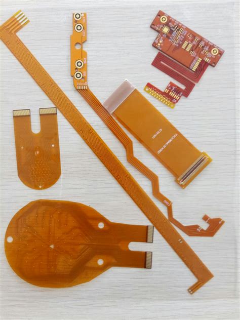
The influence and requirements of different manufacturing processes on the pads on the PCB
1. The test points must be added to the components of the chip components that are not connected to the plug-in components.
The diameter of the test points is between 1.0mm and 1.5mm, which is convenient for online tester testing. The edge of the test pad is at least 0.4 mm from the edge of the surrounding pad. The test pad has a diameter of 1mm or more and must have network properties. The center distance between the two test pads should be greater than or equal to 2.54mm. If a via is used as the measurement point, the pad must be added outside the via. Above 1mm (inclusive).
2. The location of the hole with electrical connection must be padded;
all pads must have network properties, the network without the component, the network name cannot be the same; the distance between the center of the positioning hole and the center of the test pad is more than 3mm; Other irregular shapes, but there are slots, pads, etc. that are electrically connected, and are uniformly placed in the mechanical layer 1 (refer to a slotted hole such as a single insert or a fuse).
3. Component foot pads (such as ICs, swing sockets, etc.) with dense pitches (pin spacing less than 2.0 mm) must be added if they are not connected to the hand-pad pads. The test point diameter is between 1.2mm~1.5mm, which is convenient for online tester testing.
4. If the pad pitch is less than 0.4mm, white oil should be applied to reduce the over-peak soldering.
5. The ends and ends of the patch components of the dispensing process should be designed with lead-in solder. The width of the lead-in solder is recommended to be 0.5mm, and the length is generally 2 or 3mm.
6. If there is a hand-welded component on a single panel, the tin bath should be opened, the direction is opposite to the direction of the tin, and the width of the aperture is 0.3mm to 0.8mm;
7. The spacing and size of the conductive rubber buttons should match the size of the actual conductive rubber buttons.
The PCB board connected to this should be designed as a gold finger, and the corresponding gold plating thickness should be specified (generally required to be greater than 0.05um~0.015um). ).
8. The size and spacing of the pads should match the size of the chip components.
a. When special requirements are not made, the component hole shape
the pad and the component foot shape must match, and the symmetry of the pad relative to the center of the hole is ensured (the square component foot is matched with the square component hole, the square pad; the circular component foot is matched Circular element holes, round pads), and adjacent pads are kept independent to prevent thin tin and wire drawing;
b. Adjacent parts in the same line or compatible devices with different PIN spacing
there must be separate pad holes, especially between the compatible pads of the package compatible relay, such as PCB LAYOUT can not be set separately The pad holes must be surrounded by solder resist paint.
9. When designing the multi-layer board, pay attention to the components of the metal shell. When the plug-in is in contact with the printed board, the top layer of the pad should not be opened. Be sure to cover it with green oil or silk screen oil (for example, the crystal of the two feet, 3 Only the foot of the LED).
10, PCB board design and layout should minimize the slot and opening of the printed board, so as not to affect the strength of the printed board.
11. Valuable components:
Do not place valuable components on the corners, edges, mounting holes, slots, cutting edges and corners of the PCB. These positions are high-stress areas of the printed board, which is easy to cause welding. Cracks and cracks in points and components.
12. Do not move the heavy components (such as transformers) away from the positioning holes to avoid affecting the strength and deformation of the printed board. When laying out, you should choose to place the heavier device below the PCB (and the one that finally enters the wave soldering).
13. Transformers and relays that radiate energy should be kept away from amplifiers, microcontrollers, crystal oscillators, reset circuits, and other easily disturbed devices and circuits, so as not to affect the reliability of the work.
14, for the QFP package IC (requires the use of wave soldering process), must be placed at 45 degrees, and added tin.
15. When the chip component is over-wave soldered, the heat-dissipating holes on the board and the board below the body may not be opened to prevent the PCB from over-wave soldering. The tin on the upper plate is attached to the upper plate part or the part foot, and the foreign matter inside the machine is generated when assembled in the post-engineering.
16. Large-area copper foil is required to be connected to the pad with a heat-insulating tape. In order to ensure good tin penetration, the pads of the components on the large-area copper foil are required to be connected to the pads by heat-insulating tapes. For pads that require more than 5A, the pads cannot be used;
17. In order to avoid the occurrence of misalignment and tombstoning after the device has been reflowed, the solder joints at the ends of the reflow soldering 0805 and 0805 chip components should ensure thermal symmetry. The width of the connection between the pad and the printed conductor should not be greater than 0.3mm (for asymmetric pads).