
Blind Via Manufacturing Processes in PCB Production
Abstract
Blind vias are essential structures in modern printed circuit boards (PCBs), enabling high-density interconnections between outer layers and inner layers without penetrating the entire board. As electronic devices become more compact and complex, the demand for advanced PCB manufacturing techniques has increased. This paper explores various blind via fabrication methods, including laser drilling, mechanical drilling, photo-defined processes, and sequential lamination. Each technique has distinct advantages and limitations, making them suitable for different applications. The discussion covers process details, material considerations, and industry trends to provide a comprehensive understanding of blind via manufacturing.
1. Introduction
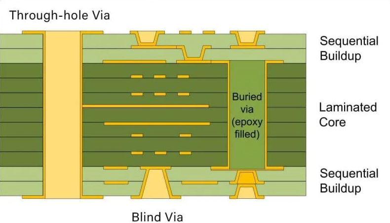
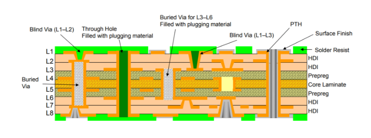
Blind vias are conductive holes that connect an outer layer of a PCB to one or more inner layers but do not pass through the entire board. They are widely used in high-density interconnect (HDI) PCBs, smartphones, wearables, and advanced computing systems. Compared to through-hole vias, blind vias save space, reduce signal interference, and improve electrical performance.
Several manufacturing methods exist for creating blind vias, each with unique process requirements. The choice of method depends on factors such as via diameter, aspect ratio, layer count, and cost constraints. This paper examines the primary blind via fabrication techniques and their applications.
2. Laser Drilling for Blind Vias
2.1 CO₂ Laser Drilling
CO₂ lasers (wavelength: 9.4–10.6 μm) are commonly used for drilling blind vias in organic PCBs. The laser ablates the dielectric material but cannot effectively remove copper, requiring a pre-etching step to expose the underlying dielectric.
Process Steps:
- Copper Etching: A photoresist is applied, and the copper layer is patterned to expose the target dielectric areas.
- Laser Ablation: The CO₂ laser removes the dielectric material, forming the via hole.
- Desmearing & Metallization: Chemical cleaning removes residue, followed by electroless copper plating to establish conductivity.
Advantages:
- High speed and precision (via diameters: 50–150 μm).
- Suitable for mass production.
Limitations:
- Cannot directly drill through copper.
- Limited to larger vias compared to UV lasers.
2.2 UV Laser Drilling
UV lasers (wavelength: 355 nm) offer finer resolution and can drill through both copper and dielectric materials, making them ideal for microvias (<100 μm).
Process Steps:
- Direct Laser Drilling: The UV laser ablates copper and dielectric sequentially.
- Cleaning & Plating: Similar to CO₂ laser processing.
Advantages:
- Higher precision (via diameters: 20–100 μm).
- No need for pre-etching copper.
Limitations:
- Slower than CO₂ lasers.
- Higher equipment costs.
3. Mechanical Drilling for Blind Vias
Mechanical drilling is a traditional method for creating blind vias, typically used for larger diameters (>200 μm).
Process Steps:
- Depth-Controlled Drilling: A CNC drill with precise depth control creates the via hole.
- Deburring & Plating: Mechanical or chemical cleaning removes debris before metallization.
Advantages:
- Lower cost for larger vias.
- Compatible with standard PCB manufacturing.
Limitations:
- Limited to larger via sizes.
- Higher risk of drill breakage in thin PCBs.
4. Photo-Defined Blind Vias
Photo-defined vias use photolithography to create blind vias in a subtractive process.
Process Steps:
- Lamination of Photosensitive Dielectric: A photosensitive resin (e.g., dry film or liquid photoimageable dielectric) is applied.
- Exposure & Development: UV light exposes the via pattern, and a developer removes unexposed areas.
- Metallization: Electroless or electrolytic plating fills the vias.
Advantages:
- High precision (via diameters: 25–75 μm).
- Suitable for ultra-HDI PCBs.
Limitations:
- Requires additional lithography steps.
- Higher material costs.
5. Sequential Lamination for Blind Vias
Sequential lamination builds PCBs layer-by-layer, creating blind vias at each stage.
Process Steps:
- Fabricate Inner Layers: Standard etching and drilling processes create inner circuits.
- Lamination & Via Formation: Each new layer is laminated, and vias are drilled (laser/mechanical) and plated.
- Repeat for Additional Layers: The process continues until the final layer is added.
Advantages:
- Enables complex multilayer PCBs.
- Compatible with various via types.
Limitations:
- Longer production time.
- Higher cost due to multiple lamination cycles.
6. Comparison of Blind Via Manufacturing Methods
| Method | Via Size (μm) | Precision | Cost | Suitable Applications |
|---|---|---|---|---|
| CO₂ Laser Drilling | 50–150 | Moderate | Medium | Consumer electronics |
| UV Laser Drilling | 20–100 | High | High | HDI, smartphones |
| Mechanical Drilling | >200 | Low | Low | Industrial PCBs |
| Photo-Defined Vias | 25–75 | Very High | High | Advanced HDI |
| Sequential Lamination | Varies | High | Very High | Aerospace, medical |
7. Emerging Trends in Blind Via Technology
- Advanced Laser Systems: Femtosecond lasers enable finer microvias with minimal thermal damage.
- Conductive Inks: Alternative metallization methods reduce reliance on electroplating.
- 3D Printed Electronics: Additive manufacturing may revolutionize PCB via formation.
8. Conclusion
Blind via fabrication is a critical aspect of modern PCB manufacturing, with multiple methods available depending on design requirements. Laser drilling (CO₂ and UV) dominates high-density applications, while mechanical drilling remains cost-effective for larger vias. Photo-defined processes and sequential lamination enable ultra-HDI and multilayer PCBs. As technology advances, new methods such as conductive ink printing and 3D PCB fabrication may further enhance blind via production.
Understanding these techniques allows PCB designers and manufacturers to select the optimal process for performance, cost, and reliability.