
How to Replace Footprints in PCB Using Altium Designer 16 (AD16)
Introduction
Altium Designer 16 (AD16) is a powerful electronic design automation (EDA) software for printed circuit board (PCB) design. One common task during PCB layout is replacing component footprints, whether due to part availability changes, design optimization, or error correction. This 2000-word guide provides a comprehensive walkthrough of footprint replacement in AD16, covering various methods and best practices.
Understanding Footprints in Altium Designer
Before replacing footprints, it’s essential to understand their role in PCB design:
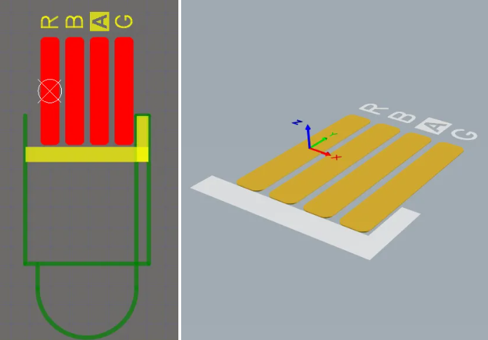
- Footprint Definition: A footprint (or PCB decal) represents the physical interface between a component and the board, including pad patterns, silkscreen outlines, and 3D models.
- Footprint-Library Relationship: Footprints are stored in library files (.PcbLib) and linked to schematic components through the schematic library (.SchLib).
- Importance of Correct Footprints: Using accurate footprints ensures proper component placement, soldering, and mechanical fit.
Method 1: Direct Footprint Replacement in PCB Editor
Step-by-Step Process:
- Open Your PCB Document: Launch AD16 and open your PCB file (.PcbDoc).
- Access Component Properties:
- Right-click on the component whose footprint you want to change
- Select “Properties” or double-click the component
- Alternatively, use the shortcut key “F11” to open the PCB Inspector panel
- Modify Footprint Information:
- In the properties dialog, locate the “Footprint” section
- Click the “…” button next to the footprint name to open the Browse Libraries dialog
- Select New Footprint:
- Browse through available libraries (Installed libraries, project libraries, or search paths)
- Select the appropriate replacement footprint
- Preview the footprint to verify its suitability
- Apply Changes:
- Click “OK” to confirm the new footprint selection
- The component will update immediately in the PCB workspace
- Adjust Component Placement (if needed):
- The new footprint may have different dimensions, requiring position adjustment
- Use the “Move” command (shortcut “M”) to reposition if necessary
Advantages:
- Quick and straightforward for individual component changes
- No schematic modification required
- Immediate visual feedback
Limitations:
- Changes made only in PCB don’t update the schematic-library linkage
- Not efficient for bulk replacements
Method 2: Updating Footprints via Schematic
For a more systematic approach that maintains synchronization between schematic and PCB:
- Open Schematic Document: Navigate to your project’s schematic sheet (.SchDoc).
- Access Component Properties:
- Double-click the component to open its properties
- Locate the “Footprint” parameter in the “Models” section
- Browse for New Footprint:
- Click “Add” or “Edit” in the Models section
- Select “Footprint” as the model type
- Browse and select the replacement footprint from available libraries
- Update PCB:
- Save schematic changes
- Open the PCB document
- Execute “Design » Update PCB Document [YourPCBName.PcbDoc]”
- Review changes in the Engineering Change Order (ECO) dialog
- Click “Execute Changes” to apply updates
Advantages:
- Maintains schematic-PCB synchronization
- Updates component parameters in both domains
- Better for design integrity
Limitations:
- Requires schematic access and modification
- Slightly more time-consuming for single components
Method 3: Batch Footprint Replacement
For replacing multiple footprints simultaneously:
- Open PCB List Panel:
- Navigate to “Panels » PCB » PCB List” or use shortcut “F12”
- Configure View:
- Set the panel to “Edit” mode
- Filter to show “Components” or specific component classes
- Select Multiple Components:
- Use standard selection techniques (click+drag, Ctrl+click)
- Or use the panel’s filtering capabilities to select components by criteria
- Edit Footprint Parameter:
- In the PCB List panel, locate the “Footprint” column
- Edit the field directly for selected components
- Or use the “Footprint Manager” (Tools » Footprint Manager)
- Verify Changes:
- Visually inspect the board for proper updates
- Check for any placement or clearance issues
Advantages:
- Efficient for global changes
- Can use filtering for selective replacement
- Maintains consistency across similar components
Limitations:
- Requires careful selection to avoid unintended changes
- May need manual adjustment of component placement afterward
Method 4: Using the Footprint Manager
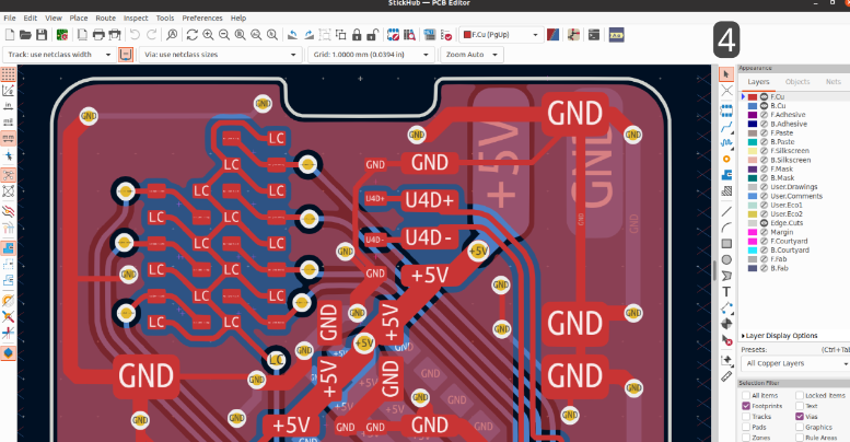
AD16’s Footprint Manager provides advanced control:
- Access Footprint Manager:
- From the PCB editor: “Tools » Footprint Manager”
- From the schematic editor: “Tools » Footprint Manager”
- Navigate Components:
- The left pane lists all components in the design
- Select components needing footprint changes
- Modify Footprint Assignments:
- Select a component and click “Edit Footprint”
- Browse and select the new footprint
- Use “Assign All Matching” for components with similar characteristics
- Review and Apply:
- Check the “Proposed Footprint” column for accuracy
- Click “Accept Changes (Create ECO)” to implement modifications
- Execute ECO:
- Review the Engineering Change Order
- Click “Execute Changes” to update the PCB
Advantages:
- Comprehensive view of all footprint assignments
- Powerful filtering and batch operations
- Maintains design synchronization
Limitations:
- More complex interface
- May be overkill for simple replacements
Best Practices for Footprint Replacement
- Verify Before Replacing:
- Always check datasheets for correct footprint dimensions
- Compare pad sizes, spacing, and outline with component requirements
- Maintain Library Links:
- Ensure replacement footprints come from managed libraries when possible
- Avoid using temporary or unverified footprints
- Check Clearances:
- After replacement, verify clearances with nearby components
- Run Design Rule Check (DRC) to identify any new violations
- Update 3D Models:
- If using 3D visualization, ensure the new footprint has an associated 3D model
- Verify mechanical fit in the enclosure if applicable
- Document Changes:
- Maintain revision notes about footprint changes
- Update BOM (Bill of Materials) if footprint change affects part numbers
- Consider Manufacturing:
- Verify that new footprints are manufacturable with your PCB fabricator’s capabilities
- Check solder mask and paste mask layers after replacement
Troubleshooting Common Issues
- Footprint Not Found:
- Verify the library containing the footprint is installed or in the search path
- Use “Libraries” panel to confirm library availability
- Pads Don’t Match:
- If pinouts don’t align, you may need to modify the schematic symbol first
- Check component orientation and pin numbering
- Update Not Reflecting:
- Ensure you’ve executed all ECOs completely
- Try refreshing the PCB view (View » Refresh or shortcut “End”)
- DRC Errors After Replacement:
- New footprint may violate spacing rules
- Adjust component placement or modify design rules if appropriate
- Broken Library Links:
- If footprints show as “Not Found,” re-establish library paths in Preferences
Advanced Techniques
- Footprint Variants:
- Create and manage different footprint versions for components
- Useful for alternate packaging options
- IPC-Compliant Footprints:
- Use AD16’s IPC Footprint Wizard to generate standardized footprints
- Ensures manufacturing compatibility
- 3D Model Integration:
- When replacing footprints, consider adding or updating 3D models
- Use “Place » 3D Body” to associate mechanical models
- Scripted Replacement:
- For complex projects, consider using Altium’s scripting engine
- Automate footprint replacement based on specific criteria
Conclusion
Replacing footprints in Altium Designer 16 is a fundamental skill for PCB designers, with multiple approaches available depending on the specific requirements. Whether making quick individual changes via the PCB editor, performing systematic updates through the schematic, or executing bulk modifications with the Footprint Manager, AD16 provides robust tools for footprint management.
By following the methods outlined in this guide and adhering to best practices, designers can efficiently modify their PCB layouts while maintaining design integrity and manufacturing reliability. Always remember to verify changes through visual inspection and DRC checks, and document modifications for future reference.
Mastering footprint replacement in AD16 not only saves time during design iterations but also contributes to producing higher quality PCB layouts that accurately reflect the intended physical implementation of electronic circuits.