
How to Handle RF Circuits in PCB Design
Introduction
Radio Frequency (RF) circuits are critical components in modern electronics, enabling wireless communication, radar systems, and IoT devices. However, designing a printed circuit board (PCB) with RF circuits presents unique challenges due to high-frequency signal integrity, electromagnetic interference (EMI), and impedance matching requirements. Proper PCB layout techniques are essential to ensure optimal performance, minimize noise, and prevent signal degradation.
This article explores best practices for handling RF circuits in PCB design, covering key considerations such as material selection, grounding, trace routing, shielding, and testing.
1. Choosing the Right PCB Material
The substrate material significantly impacts RF circuit performance. Standard FR-4 is suitable for low-frequency applications but may introduce excessive dielectric losses at higher frequencies. For RF designs, consider specialized materials such as:
- Rogers RO4000 Series: Low-loss materials with stable dielectric constants for high-frequency applications.
- Teflon (PTFE): Excellent high-frequency performance but more expensive and harder to manufacture.
- Isola IS680: A cost-effective alternative for RF and microwave circuits.
Key parameters to evaluate include:
- Dielectric Constant (Dk): Affects signal propagation speed and impedance.
- Loss Tangent (Df): Determines signal attenuation; lower values reduce losses.
- Thermal Stability: Ensures consistent performance under temperature variations.
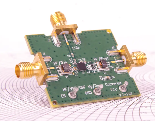
2. Proper Grounding Techniques
Grounding is crucial in RF PCB design to minimize noise and EMI. Poor grounding can lead to ground loops, parasitic capacitance, and signal interference.
a. Use a Solid Ground Plane
A continuous ground plane beneath RF traces reduces inductance and provides a low-impedance return path. Avoid splitting the ground plane under RF sections to prevent impedance discontinuities.
b. Implement Star Grounding
For mixed-signal designs (RF + digital/analog), use a star grounding scheme where all ground connections meet at a single point to avoid ground loops.
c. Avoid Ground Stubs
Unused ground connections (stubs) can act as antennas, radiating noise. Ensure all ground vias are placed close to signal paths.
3. RF Trace Routing Best Practices
a. Controlled Impedance Traces
RF signals require precise impedance matching (typically 50Ω or 75Ω). Use PCB calculators or simulation tools (e.g., ADS, HFSS) to determine trace width and spacing based on dielectric properties.
b. Minimize Trace Lengths
Long traces introduce parasitic inductance and capacitance, degrading signal quality. Keep RF traces as short as possible, especially for high-frequency signals (>1GHz).
c. Avoid Sharp Corners
Right-angle bends cause impedance discontinuities and reflections. Use 45° bends or curved traces for smoother transitions.
d. Differential Pair Routing
For differential RF signals (e.g., LVDS, USB), maintain consistent spacing and length matching to minimize skew and common-mode noise.
4. Power Supply Decoupling
RF circuits are sensitive to power supply noise. Proper decoupling ensures stable voltage delivery:
- Place decoupling capacitors (e.g., 0.1µF, 1nF) close to RF ICs.
- Use multiple capacitor values to filter a wide frequency range.
- Implement ferrite beads for additional noise suppression.
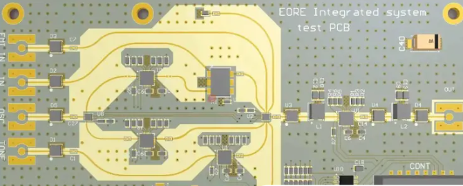
5. Shielding and EMI Mitigation
a. RF Shielding Cans
Metal enclosures (shielding cans) isolate RF components from external interference. Ensure proper grounding of shields to avoid antenna effects.
b. Partitioning the PCB
Separate RF, analog, and digital sections to prevent crosstalk. Use guard traces or moats (isolated ground regions) for critical RF signals.
c. Via Fencing
A row of grounded vias around RF traces acts as a barrier to reduce EMI radiation.
6. Component Placement and Thermal Management
a. Strategic Component Layout
- Place RF components first, minimizing trace lengths.
- Keep sensitive components (e.g., oscillators, filters) away from noisy sources (switching regulators, digital ICs).
b. Thermal Considerations
High-power RF circuits (e.g., PAs) generate heat. Use thermal vias, heatsinks, or metal-core PCBs for efficient heat dissipation.
7. Simulation and Testing
Before fabrication, simulate the design using tools like:
- Keysight ADS: For RF circuit and EM simulation.
- CST Studio Suite: For 3D electromagnetic analysis.
- Altium Designer: For impedance calculations and signal integrity checks.
Post-fabrication testing includes:
- Vector Network Analyzer (VNA): Measures S-parameters (return loss, insertion loss).
- Spectrum Analyzer: Detects unwanted emissions and harmonics.
- Time-Domain Reflectometry (TDR): Identifies impedance mismatches.
Conclusion
Designing PCBs for RF circuits requires careful attention to material selection, grounding, trace routing, and EMI control. By following these best practices, engineers can achieve optimal RF performance, minimize signal loss, and ensure reliable operation in high-frequency applications. Advanced simulation and testing further validate the design, reducing costly revisions and improving time-to-market.
As wireless technology evolves, mastering RF PCB design remains essential for next-generation communication systems.