
Skip to content
Andwin Circuits
  • Home
  • ProductsExpand
    • HDI multilayer PCB
    • Rigid Flex PCB
    • Flex pcb
    • Special PCBExpand
      • High Frequency PCBExpand
        • Rogers RO4350B PCB
        • Rogers RO4003 pcb
        • Rogers RO3003 PCB
        • Rogers 5880 PCB
        • DICLAD 527 PCB
        • Taconic TLX series
        • Taconic TLX-8 RF PCB
        • Taconic TLX-9 RF PCB
      • High speed pcbExpand
        • Megtron 6 High Speed PCB
        • TU-872 SLK Sp High Speed
      • High TG PCBExpand
        • SHENGYI SH260 PCB
        • ISOLA 370HR PCB
        • ISOLA IS410 PCB
        • ISOLA IS420 PCB
      • Heavy copper PCB
      • Copper coin pcb
      • Copper inlay PCB
    • Metal Core PCBExpand
      • Copper core pcb
      • Aluminum PCB
      • 2 Layers Aluminum PCB
      • Direct thermal MCPCB
      • 2 Layers Direct Thermal
    • Ceramic PCBExpand
      • DPC ceramic PCB
      • DBC ceramic PCB
      • Thick film Ceramic PCB
      • Al2O3 Alumina PCB
      • AIN ALN ceramic PCB
      • IGBT Ceramic PCB
  • ServiceExpand
    • PCB Assembly
    • Quick turn PCB assembly
    • PCBA conformal coating
  • IndustryExpand
    • Telecommunication
    • IoT and Wireless
    • Industrial Control
    • Thermal management
    • Power and Energy
    • IC test board
    • Automative
    • Medical
  • CapabilityExpand
    • Rigid PCB
    • Rigid flex PCB
    • Metal core PCB
    • PCB Assembly
  • TechnologyExpand
    • Blogs
    • Via in pad
    • PCB E-test
    • PCB stack up
    • MCPCB panelization
    • Controlled impedance PCB
  • AboutExpand
    • About us
    • Certification
    • Factory Tour
  • Contact
Andwin Circuits
Home / Blogs / What is the significance of each layer in PCB design?

What is the significance of each layer in PCB design?

ByGrace September 11, 2025March 31, 2026

1.Signal layers

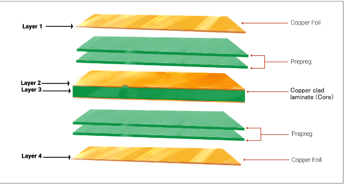
Altium Designer can provide up to 32 signal layers,including the top layer,bottom layer,and mid-layer.Each layer can be connected to each other through via,blind vias,and buries vias.

(1)Top signal Layer

Also known as the component layer,it is mainly uesd to place components.For double-layer and multi-layer boards,it can be used to arrange wires or copper.

(2)Bottom signal layer

Also know as the soldering layer,it is mainly used for wiring and soldering.For double-layer and multi-layer board,it can be uesd to place components.

(3)Mid-layers

There can be up to 30 layers,In multi-layer boards,it is used to arrange signal line.Power line and ground lines are not included here.
Contact us for PCB quote now |

2.Internal Power Planes

Usually referred to as internal power layers,they only appear in multi-layer boards.The number of PCB Layers generally refers to the sum of the signal layers and internal power layers,Similar to the signal layers,internal power layers and internal power layers and signal layers can be connected to each other through through holes,blind holes and buries holes.

3.Silkscreen layers

A pcb board can have up to two silkscreen layers namely the top silkscreen layers,namely the top silkscreen layer(Top overlay)and the bottom silkscreen layer(Bottom Overlay).They are usually white and are mainly used to place printed information,such as the outline and marking of components.various annotation characters etc.to facilitate component soldering and circuit inspection of PCB.

(1)Top Silkscreen Layer

Used to mark the Projection outline of component,component numbers,nominal values or models,and various annotation characters.

(2)Bottom Overlay

Similar to the top silkscreen layer,if all marking are already included in the top silkscreen layer,the bottom silkscreen layer can be closed.

4.Mechanical layers

The mechanical layer is generally used to place instructive information about aboard manufacturing and assembly methods such as PCB dimensions,size marking,data sheets via information,assembly instruction,etc.This information varies depending on the requirements of the design company or PCB manufacturer.The following examples illustrate our common methods.

Mechanical 1:Generally used to draw the PCB outline,representing its mechanical shape, hence the name”Outline Layer”;

Mechanical 2;Used to place the PCB fabrication process requirement table,including information such as dimensions board material and board layers;

Mechanical 13 & Mechanical 15: Dimensional information for most components in the ETM library, including their 3D models; for simplicity, this layer is not displayed by default;

Mechanical 16: Footprint information for most components in the ETM library, useful for estimating PCB dimensions in the early stages of a project; for simplicity, this layer is not displayed by default and is black.

5.Mask Layers

    Altum Designer provides two types of mask layers: solder mask and paste mask, each with a top layer and a bottom layer.

    Post navigation

    Previous Previous
    Methods for Exporting Coordinate Date from PCB software
    NextContinue
    Andwin PCB Manufacturer

    Search

    Search

    Products

    • HDI Multilayer PCB
    • Rigid Flex PCB
    • Flex pcb
    • High Frequency PCB
    • High speed pcb
    • Heavy copper PCB
    • Metal Core PCB
    • Ceramic PCB

    Address

    Andwin Circuits Co.,Limited
    Email: sales@andwinpcb.com
    Tel: +86 755 2832 9394
    Fax:+86 755 2992  6717
    ADD:1-2F-1217,HouDeQun Industrial park,
    NanTing RD NO.56,ShaJing,BaoAn,Shenzhen 518104,GuangDong,China

    Products

    • HDI Multilayer PCB
    • Rigid Flex PCB
    • Flex pcb
    • High Frequency PCB
    • High speed pcb
    • Heavy copper PCB
    • Metal Core PCB
    • Ceramic PCB

    Technology

    • Blogs
    • Via in pad
    • PCB E-test
    • PCB stack up
    • Metal core PCB panelization
    • Controlled impedance PCB

    CERTIFICATION

    Certification >>


    Copyright© 2003 - 2026 Andwin | All Rights Reserved | Powered by Andwin

    Scroll to top
    • Home
    • Products
      • HDI multilayer PCB
      • Rigid Flex PCB
      • Flex pcb
      • Special PCB
        • High Frequency PCB
          • Rogers RO4350B PCB
          • Rogers RO4003 pcb
          • Rogers RO3003 PCB
          • Rogers 5880 PCB
          • DICLAD 527 PCB
          • Taconic TLX series
          • Taconic TLX-8 RF PCB
          • Taconic TLX-9 RF PCB
        • High speed pcb
          • Megtron 6 High Speed PCB
          • TU-872 SLK Sp High Speed
        • High TG PCB
          • SHENGYI SH260 PCB
          • ISOLA 370HR PCB
          • ISOLA IS410 PCB
          • ISOLA IS420 PCB
        • Heavy copper PCB
        • Copper coin pcb
        • Copper inlay PCB
      • Metal Core PCB
        • Copper core pcb
        • Aluminum PCB
        • 2 Layers Aluminum PCB
        • Direct thermal MCPCB
        • 2 Layers Direct Thermal
      • Ceramic PCB
        • DPC ceramic PCB
        • DBC ceramic PCB
        • Thick film Ceramic PCB
        • Al2O3 Alumina PCB
        • AIN ALN ceramic PCB
        • IGBT Ceramic PCB
    • Service
      • PCB Assembly
      • Quick turn PCB assembly
      • PCBA conformal coating
    • Industry
      • Telecommunication
      • IoT and Wireless
      • Industrial Control
      • Thermal management
      • Power and Energy
      • IC test board
      • Automative
      • Medical
    • Capability
      • Rigid PCB
      • Rigid flex PCB
      • Metal core PCB
      • PCB Assembly
    • Technology
      • Blogs
      • Via in pad
      • PCB E-test
      • PCB stack up
      • MCPCB panelization
      • Controlled impedance PCB
    • About
      • About us
      • Certification
      • Factory Tour
    • Contact
    Search