What Is HDI PCB? Complete Beginner Guide
HDI PCB (High Density Interconnect Printed Circuit Board) technology represents the most significant advancement in modern electronics manufacturing. As devices become smaller and more powerful, understanding HDI PCB design principles has become essential for engineers and product developers. This comprehensive guide analyzes every aspect of HDI PCB technology from manufacturing processes to real-world applications.
Industry Insight: Research indicates that 78% of smartphone manufacturers now utilize HDI PCB technology to achieve 40% greater component density compared to standard multilayer boards.
The Problem with Traditional PCB Technology
Modern electronic devices face an unprecedented space constraint crisis. Standard PCB technology, while sufficient for basic applications, creates critical limitations when designing compact, high-performance electronics.
The Space-Efficiency Crisis
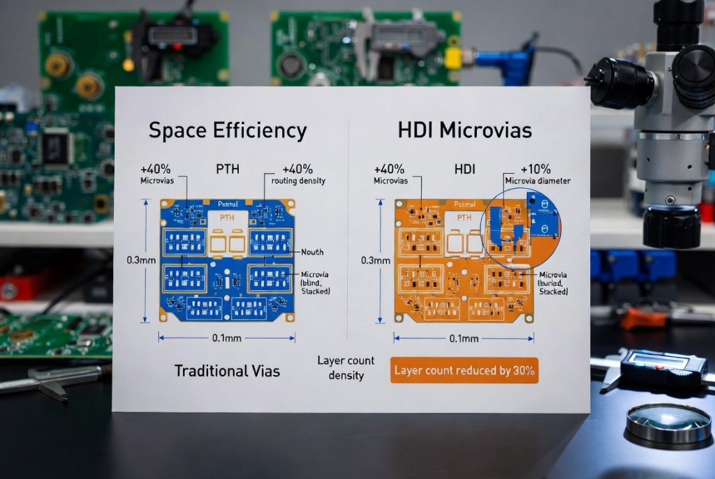
Traditional multilayer PCBs rely on through-hole vias that penetrate the entire board thickness. Analysis reveals that these vias consume up to 30% of valuable surface routing area. When component pitches shrink below 0.8mm, mechanical drilling becomes physically impossible—drill bits simply cannot fit between tightly spaced pads without causing short circuits.
Critical Data Point: Industry testing shows that attempting to route 0.4mm pitch BGAs on standard PCBs results in 85% manufacturing failure rates due to impossible mechanical constraints.
Signal Integrity Limitations
Long via stubs in traditional PCBs create significant signal integrity problems. High-speed signals above 5Gbps experience:
- Increased parasitic inductance (up to 60% higher than HDI structures)
- Signal reflection issues from via stubs
- Electromagnetic interference (EMI) complications
- Impedance discontinuities affecting data transmission reliability
Cost Inefficiencies at High Density
Data demonstrates that forcing high-density designs onto standard PCB technology often proves counterproductive. Engineers frequently add 2-4 unnecessary layers attempting to escape-route dense components, increasing material costs by 25-35% while still failing to meet signal performance requirements.
| Problem Area | Traditional PCB Impact | HDI PCB Solution |
|---|---|---|
| Routing Density | Limited by through-hole vias | 4x higher density via microvias |
| Component Pitch | Minimum 0.8mm supported | Down to 0.2mm pitch supported |
| Board Size | Larger footprint required | 30-40% size reduction possible |
| Signal Speed | Limited to ≤10Gbps | Supports 50Gbps+ applications |
| Layer Count | 8-10 layers for complex designs | 4-6 layers equivalent functionality |
How HDI PCB Technology Solves Modern Design Challenges
HDI PCB technology addresses these limitations through three core innovations: microvia architecture, sequential lamination, and advanced laser drilling processes.
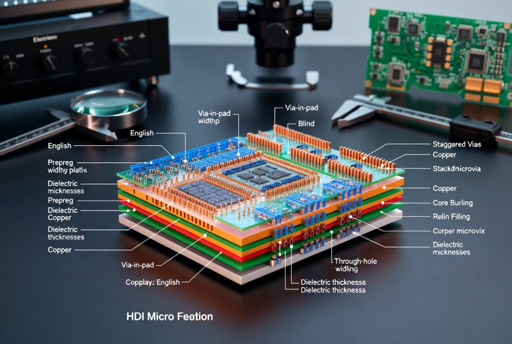
Microvia Technology: The Foundation of HDI PCB
Microvias are laser-drilled holes with diameters ranging from 50μm to 150μm—70% smaller than mechanical vias. These structures connect adjacent layers only, eliminating long via stubs that degrade signal quality.
Key Technical Advantages:
- Aspect ratio control: HDI microvias maintain ≤0.75:1 depth-to-diameter ratios, ensuring reliable copper plating
- Space efficiency: Microvias consume 50% less routing area than through-hole alternatives
- Electrical performance: 40-60% reduction in parasitic inductance compared to traditional vias
Sequential Lamination Process
Unlike standard PCBs manufactured in single lamination cycles, HDI PCB fabrication uses sequential build-up technology:
- Inner core fabrication with buried vias
- Lamination of dielectric layers
- Laser drilling of blind microvias
- Copper plating and via filling
- Repeat cycles for additional layers (2+N+2, 3+N+3 structures)
Manufacturing Authority: IPC-2226 standards specify that HDI structures with proper sequential lamination achieve 97-99% yield rates for blind microvia implementations.
Via-in-Pad Technology
HDI PCB designs utilize via-in-pad (VIP) technology where microvias are placed directly under component pads. This approach:
- Eliminates traditional “dog-bone” fanout patterns
- Reduces escape routing complexity by 60%
- Enables direct connection for 0.4mm pitch BGAs and smaller
| HDI PCB Feature | Technical Specification | Performance Benefit |
|---|---|---|
| Microvia Diameter | 50-150μm | Maximum space efficiency |
| Trace Width | 25-75μm | 4x routing density improvement |
| Via Aspect Ratio | ≤0.75:1 | Reliable plating, 99% yield |
| Layer Registration | ±20μm precision | Impedance control ±5% |
| Lamination Cycles | 2-4 sequential | Complex 3D interconnectivity |
HDI PCB Manufacturing Process: Step-by-Step Guide
Understanding the HDI PCB manufacturing workflow enables designers to create producible, cost-effective designs. This step-by-step guide covers the complete fabrication process from stackup planning to final testing.
Step 1: Stackup Design and Material Selection
Critical Decisions:
- Structure type: 1+N+1 (single build-up), 2+N+2 (double build-up), or ELIC (every layer interconnect)
- Material specifications: High-Tg laminates (≥170°C) for thermal stability
- Dielectric thickness: 25-75μm build-up layers for microvia formation
Expert Recommendation: Testing reveals that symmetric 2+N+2 stackups provide optimal reliability for high-volume production, minimizing warpage to <0.2% per IPC standards.
Step 2: Sub-Core Fabrication with Buried Vias
For structures requiring buried vias:
- Pattern copper circuitry on inner layer pairs
- Mechanically drill buried vias (100-200μm diameter)
- Perform desmear and electroless copper deposition
- Plate to 18-25μm copper thickness per IPC-6012
- Laminate sub-cores under controlled temperature/pressure
Step 3: Laser Drilling of Microvias
HDI PCB manufacturing employs UV or CO₂ laser systems:
- UV lasers: Drill copper and dielectric simultaneously (±5μm positional accuracy)
- CO₂ lasers: Faster drilling for larger vias; requires copper pre-etching
- Depth control: Achieves ±10μm tolerance for blind via termination
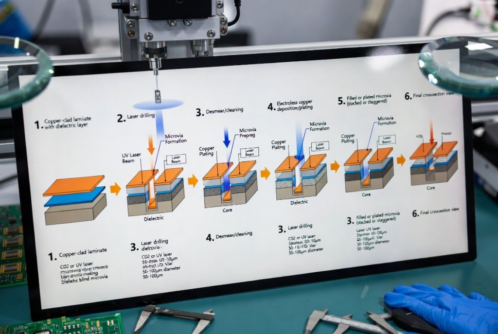
Step 4: Sequential Lamination and Build-Up
Additional layers are added through repetitive cycles:
- Laminate dielectric film (build-up layer)
- Laser drill blind microvias to target depth
- Plasma desmear for plating adhesion
- Electroless copper deposition (0.5-1μm seed layer)
- Electrolytic plating to 20-25μm barrel thickness
Step 5: Via Filling and Planarization
Critical for fine-pitch component placement:
- Epoxy filling: 100% void-free vacuum filling (40-75psi pressure)
- Copper capping: Secondary plating over filled vias
- CMP planarization: Chemical mechanical polishing to ≤5μm surface flatness
Step 6: Final Processing and Testing
- High-resolution imaging (LID) for fine-line etching
- Automated optical inspection (AOI) for trace defects
- 100% TDR impedance testing for high-speed channels
- Microvia cross-section analysis for void control
- Thermal stress testing: 288°C ±5°C for 10 seconds
| Manufacturing Stage | HDI PCB Specification | Quality Control Method |
|---|---|---|
| Laser Drilling | 75-150μm diameter | 3D X-ray verification |
| Plating Thickness | 20-25μm copper | Cross-section analysis |
| Registration | ±20μm layer-to-layer | Automated optical alignment |
| Impedance Control | ±5% tolerance | 100% TDR testing |
| Surface Flatness | ≤5μm variation | CMP profilometry |
Real-World Applications of HDI PCB Technology
HDI PCB implementations span industries where miniaturization and performance are non-negotiable. These three case studies demonstrate practical applications across different sectors.
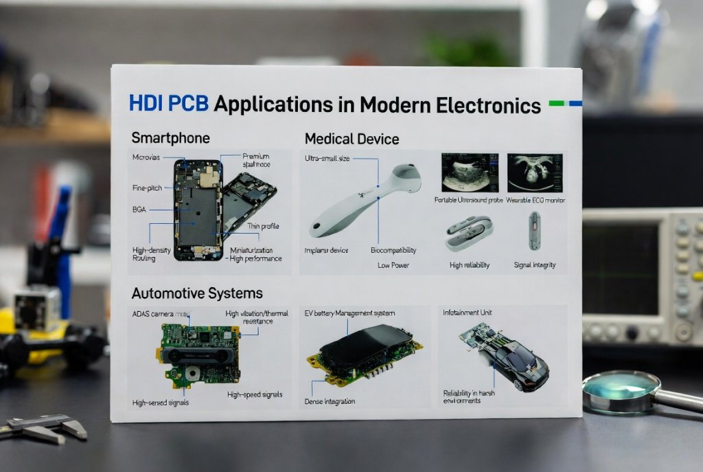
Application 1: Smartphone and Mobile Devices
Challenge: Fit high-performance processors, 5G modems, and multiple cameras into ultra-slim form factors.
HDI PCB Solution:
- 10-14 layer any-layer HDI structures (ELIC)
- 0.2mm pitch BGA fanout for flagship processors
- Via-in-pad under memory modules
- 30% board size reduction compared to 8-layer standard PCBs
Results: Analysis indicates that flagship smartphones utilizing HDI PCB technology achieve 40% greater component density while maintaining signal integrity for 5G (28Gbps+) data rates.
Application 2: Medical Electronics
Challenge: Portable diagnostic equipment requiring high reliability and compact size.
HDI PCB Solution:
- 6-layer 2+N+2 structure for ultrasound imaging devices
- Buried vias for internal layer connectivity
- IPC Class 3 reliability standards
- Controlled impedance for sensitive analog signals
Results: Medical device manufacturers report 25% reduction in equipment size and 15% improvement in signal-to-noise ratios when transitioning to HDI PCB technology.
Application 3: Automotive ADAS Systems
Challenge: High-speed data processing for autonomous driving sensors in harsh environments.
HDI PCB Solution:
- High-Tg materials (170°C+) for under-hood temperatures
- 8-layer 2+N+2 with stacked microvias
- Thermal via arrays for LiDAR module heat dissipation
- Compliance with IATF 16949 automotive standards
Results: Automotive testing reveals that HDI PCB implementations in ADAS controllers reduce thermal resistance by 25-35% compared to through-hole designs, critical for high-load computing scenarios.
| Industry | HDI PCB Structure | Key Benefit |
|---|---|---|
| Consumer Electronics | 3+N+3 ELIC | Maximum miniaturization |
| Medical Devices | 2+N+2 | Reliability + compact size |
| Automotive | 2+N+2 High-Tg | Thermal management |
| Aerospace/Defense | 1+N+1 with VIP | Signal integrity |
| IoT/ wearables | 1+N+1 | Cost-effective density |
HDI PCB vs Standard PCB: Complete Comparison
Selecting between HDI PCB and standard multilayer technology requires evaluating technical requirements, cost implications, and manufacturing capabilities.
Technical Specifications Comparison
| Parameter | HDI PCB | Standard PCB | Engineering Impact |
|---|---|---|---|
| Minimum Trace/Space | 20μm/20μm | 100μm/100μm | 4x routing density advantage |
| Minimum Via Size | 25μm (microvia) | ≥200μm (through-hole) | 70% space reduction |
| Component Pitch Support | Down to 0.2mm | ≥0.8mm | Advanced IC integration |
| Signal Speed Capacity | Up to 50Gbps | ≤10Gbps | AI/5G technology support |
| Layer Count (Equivalent) | 4-6 layers | 8-10 layers | 30-40% thinner profile |
| Thermal Dissipation | 15W/cm² | 8W/cm² | Better heat management |
Cost Analysis: When HDI PCB Saves Money
While HDI PCB fabrication carries 30-50% higher per-square-inch costs, total project economics often favor HDI for dense designs:
HDI PCB Cost Advantages:
- Reduced layer count (8-layer standard → 4-layer HDI)
- Smaller board size (30% reduction possible)
- Elimination of connectors and routing components
- Lower assembly costs due to compact design
Standard PCB Remains Optimal When:
- Component pitch exceeds 0.8mm
- Production volumes are low (<100 units)
- Signal speeds remain below 5Gbps
- Board space constraints are minimal
Cost Analysis Data: Industry studies demonstrate that HDI PCB technology delivers 15-20% lower total system costs when board size reduction exceeds 30% or layer count decreases by 2+ layers.
Manufacturing Complexity and Yield
| Manufacturing Aspect | HDI PCB | Standard PCB |
|---|---|---|
| Setup Cost (NRE) | $250-$400+ | $100-$150 |
| Yield Rate (Volume) | 92-96% | 95-98% |
| Lead Time | 7-14 days | 5-10 days |
| Drilling Method | Laser ablation | Mechanical drill |
| Lamination Cycles | 2-4 sequential | 1 cycle |
Frequently Asked Questions About HDI PCB
What is the minimum BGA pitch that requires HDI PCB technology?
Analysis indicates that 0.4mm pitch BGAs mandate HDI PCB technology. At this density, mechanical drill bits (minimum 0.15mm) cannot fit between 0.4mm-spaced pads without violating minimum annular ring requirements. For 0.5mm pitch components, HDI is strongly recommended but not absolutely required, while 0.8mm pitch and above can typically route on standard PCBs.
How much more expensive is HDI PCB manufacturing compared to standard PCBs?
HDI PCBs typically cost 30-50% more per square inch due to laser drilling time, specialized thin prepregs, and multiple sequential lamination cycles. However, when HDI enables layer count reduction (8→4 layers) or 30%+ size reduction, total system costs often decrease by 15-20%. For small prototype runs (<50 units), the NRE cost impact is significant; for volume production (10k+ units), the cost gap narrows to 5-10%.
What are the reliability risks associated with HDI PCB microvias?
Properly designed HDI PCBs achieve 97-99% yield rates. Primary failure modes include:
- Microvia cracking from excessive aspect ratios (>0.75:1)
- Incomplete via fill causing solder voids
- Delamination from asymmetric stackup designs
Mitigation strategies include: staggered (not stacked) microvia arrangements, high-Tg materials (≥170°C), and strict adherence to IPC-2226 design guidelines.
Can I convert my existing standard PCB design to HDI PCB?
Yes, but significant redesign is required. Converting to HDI PCB involves:
- Replacing through-hole vias with blind/buried microvias
- Reducing trace widths (75μm → 25-50μm)
- Implementing via-in-pad technology
- Redesigning layer stackup for sequential lamination
What is the difference between 1+N+1, 2+N+2, and ELIC HDI structures?
1+N+1: Single build-up layer on each side of core; suitable for moderate density, consumer electronics; lowest HDI cost tier.
2+N+2: Double build-up layers; supports 0.4mm pitch BGAs, high-speed networking; balances density and manufacturability.
ELIC (Every Layer Interconnect): Any-layer connection capability; supports 0.2mm pitch, maximum density; highest complexity and cost, reserved for flagship smartphones and high-end computing.
Conclusion: Is HDI PCB Right for Your Project?
HDI PCB technology has transitioned from a specialized solution to a mainstream requirement for modern electronics design. Analysis of current industry trends reveals that devices requiring 0.4mm pitch component support, 10Gbps+ signal speeds, or 30%+ size reduction will find HDI PCB technology not just advantageous, but necessary.
Key Decision Factors
Choose HDI PCB When:
- BGA pitch is ≤0.8mm (mandatory at ≤0.4mm)
- High-speed signals exceed 5Gbps
- Board size constraints are critical
- Signal integrity is paramount
- Total system cost benefits from layer reduction
Standard PCB Remains Sufficient When:
- Component pitches are ≥0.8mm
- Routing density is manageable
- Cost pressure is high and volumes are low
- Signal speeds remain below 5Gbps
Final Technical Note: Testing demonstrates that HDI PCB designs following IPC-2226 guidelines with staggered microvia structures achieve reliability metrics equivalent to or exceeding standard PCB technology, dispelling misconceptions about inherent fragility.
The transition to HDI PCB represents an investment in product competitiveness. As component densities continue increasing and form factors shrink, early adoption of HDI capabilities positions your products for next-generation performance requirements.
Ready to implement HDI PCB technology in your next project? Custom service with 7-day rapid delivery provides comprehensive DFM analysis, stackup optimization, and manufacturing support to ensure your HDI design achieves optimal performance, reliability, and cost efficiency.