
How to Design Flawless Flexible Connections for Wearable Medical Rigid-Flex PCBs
A smart insulin pump fails to deliver a life-saving dose. A continuous ECG monitor drops critical cardiac data. In the realm of wearable medical devices, these aren’t just technical glitches—they are catastrophic failures that lead to FDA recalls, massive financial losses, and compromised patient safety. The culprit behind these failures is rarely the core microprocessor; more often than not, it is a micro-fracture in the flexible connection of the rigid-flex printed circuit board (PCB).
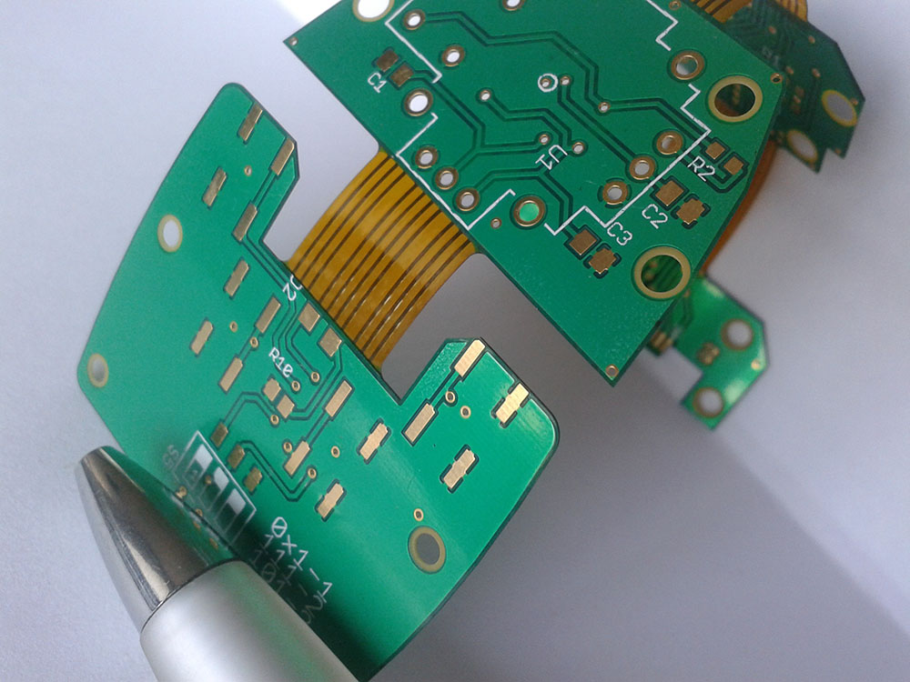
As medical wearables become smaller and more sophisticated, hardware engineers face immense “reliability anxiety.” You are tasked with cramming high-frequency sensors, Bluetooth modules, and power management into a device that must constantly bend, twist, and stretch with the human body.
In this comprehensive engineering guide, we will dissect the mechanics of stress relief in the rigid-flex transition zone, demystify IPC-2223 bending calculations, and provide proven layout strategies to prevent trace cracking and delamination. Whether you are battling electromagnetic interference (EMI) or trying to maximize flex cycle life, this guide will help you design highly reliable custom Rigid-Flex PCBs that pass rigorous medical certifications (ISO 13485, FDA).
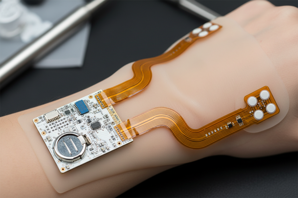
Understanding Wearable Medical Rigid-Flex PCBs: The Basics
The human body is an incredibly hostile environment for electronics. A wearable device attached to a patient’s wrist or chest is subjected to continuous kinetic stress, temperature fluctuations, and corrosive elements like sweat.
In traditional consumer electronics, a flex circuit might only be bent once during assembly. In medical wearables, the flexible connections act as the central nervous system, transmitting microvolt-level biosignals while enduring thousands of dynamic bending cycles.
If the design does not account for mechanical stress distribution, the copper traces will work-harden and snap, or the layers will separate (delamination). Designing for medical applications requires a paradigm shift: you must stop thinking of the PCB as a rigid static board and start treating it as a dynamic, electromechanical fabric. Every via placement, copper weight decision, and material selection must be strictly governed by standards like IPC-2223 (Sectional Design Standard for Flexible Printed Boards) to ensure zero-failure operation in the field.
Core Concepts Simplified: The Mechanics of Bending
To engineer a reliable wearable device, we must first translate complex mechanical physics into practical PCB layout rules. Let’s break down the core concepts using plain English and relatable analogies.
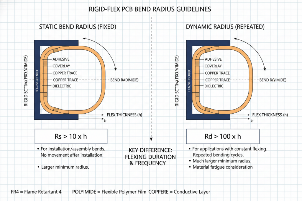
Dynamic vs. Static Bending
Not all bends are created equal. The required bend radius (how tightly you can fold the flex board without breaking it) depends entirely on how the device is used.
- Dynamic Bending (The “Door Hinge”): Imagine a door hinge that opens and closes continuously. In wearables like smart finger rings or joint-monitoring bands, the flex circuit bends constantly with the user’s movement. For dynamic applications, the copper must be extremely thin, and the bend radius must be large (typically 100x the thickness of the flex circuit) to survive tens of thousands of cycles.
- Static Bending (The “Origami Box”): Imagine folding a cardboard box once to fit it into a tight space. This is “Bend-to-Install.” The flex circuit is folded during assembly and remains stationary inside the device casing (e.g., a compact hearing aid). Because it only bends once or twice, you can use a much tighter bend radius (typically 10x the thickness of the flex circuit).
The Transition Zone (The “Shock Absorber”)
The most vulnerable part of a rigid-flex PCB is the Transition Zone—the exact line where the soft, flexible polyimide (PI) meets the hard, rigid FR4 material.
Think of bending a credit card back and forth; it always snaps at the fulcrum point. To prevent the flex circuit from tearing like paper at this hard edge, engineers must design “shock absorbers” (strain relief) to distribute the mechanical stress safely across a wider area.
Core Concept Comparison Table
| Feature | Static Bending (Bend-to-Install) | Dynamic Bending (Continuous Flexing) |
|---|---|---|
| Use Case in Wearables | Fitting PCB into a compact hearing aid shell. | Joint monitors, smart patches, wristbands. |
| IPC-2223 Minimum Bend Radius | 10x the flex circuit thickness. | 100x the flex circuit thickness. |
| Preferred Copper Type | Electrodeposited (ED) or Rolled Annealed (RA). | Strictly Rolled Annealed (RA) Copper. |
| Layer Count in Flex Area | Up to 4-6 layers (can be slightly thicker). | Max 1-2 layers (must be extremely thin). |
| Cycle Life Expectancy | < 10 cycles. | 10,000 to 1,000,000+ cycles. |
Step-by-Step Guide: Designing for Zero-Failure Connections
Achieving high yield and field reliability requires meticulous attention to detail during the CAD layout phase. Here is your actionable engineering guide to designing flawless flexible connections.
Mastering the Transition Zone Stress Relief
Delamination at the rigid-flex interface is the number one cause of manufacturing rejection. To prevent this, you must implement structural safeguards.
- The Polyimide (PI) Overlap: Never let the flexible coverlay end exactly flush with the rigid FR4 edge. The coverlay must extend (overlap) into the rigid section by at least 1.0mm to 2.0mm. This anchors the flexible materials securely inside the rigid board, preventing them from peeling apart.
- Strain Relief Fillets (Epoxy Beads): Apply a bead of flexible epoxy (often called a strain relief fillet) exactly at the transition line. This acts as a mechanical buffer, absorbing the shock and preventing the sharp FR4 edge from acting like a guillotine against the polyimide.
- Keep-Out Zones for Vias: Never place Plated Through Holes (PTH) or vias within 2.54mm (100 mils) of the transition line. Vias create mechanical weak points. Bending stress will concentrate around these holes, leading to immediate barrel cracking.
Trace Routing Tactics for High Flexibility
How you draw your copper traces determines whether your device will last five years or five minutes.
- Teardrop Traces (Reinforced Seams): When a narrow flexible trace connects to a wider pad or via, the abrupt change in width creates a stress concentration point. Add “teardrops” (extra copper tapering smoothly from the pad to the trace). This is exactly like adding reinforced stitching to the stress points of a garment, preventing the trace from tearing away from the pad during bending.
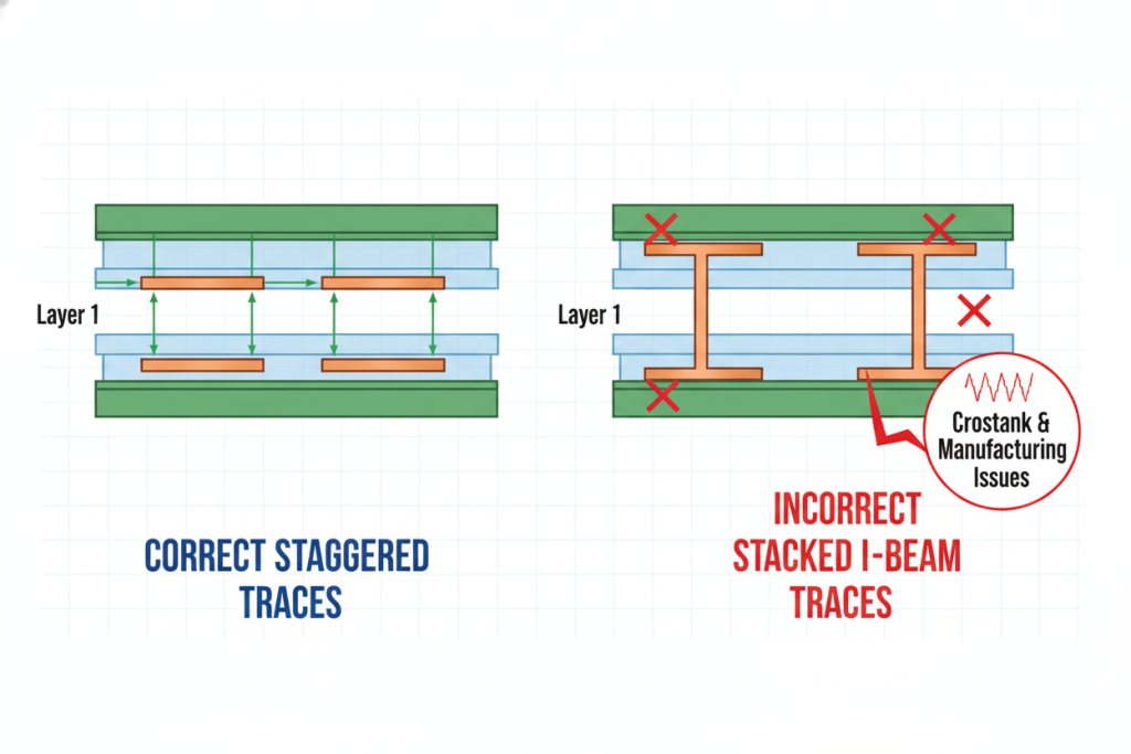
- Staggered Traces (Avoiding the I-Beam Effect): If you have a double-sided flex circuit, never route the top layer traces directly over the bottom layer traces. When stacked perfectly on top of each other, they create a rigid “I-beam” structure that resists bending and causes the outer trace to snap under tension. Instead, stagger them (offset them) like alternating bricks. This allows the flex board to bend smoothly without creating localized hard spots.
Wearable Rigid-Flex Material Specification Table
| Material Component | Recommended Spec for Medical Wearables | Why it Matters |
|---|---|---|
| Copper Type | Rolled Annealed (RA) Copper | The grain structure of RA copper runs horizontally, making it vastly superior for repeated bending compared to ED copper. |
| Adhesive | Adhesiveless Polyimide (PI) Base | Acrylic adhesives crack and harden over time. Adhesiveless PI is thinner, more flexible, and handles high temperatures better. |
| Coverlay | 0.5 mil to 1.0 mil Polyimide | Thinner coverlays reduce overall thickness, exponentially increasing the dynamic bend cycle life. |
EMC & Signal Integrity in Flexible Medical Devices
Medical sensors measure extremely weak signals (like microvolt ECG heartbeats). These signals are highly susceptible to electromagnetic interference (EMI) from the device’s own Bluetooth antenna or external hospital equipment. It is like trying to hear a whisper in a crowded, noisy room.
You need a ground plane to shield these signals, but a solid sheet of copper will make the flex circuit too stiff to bend. The solution is Cross-hatched Ground Planes.
Instead of solid copper, design the ground plane like a “fishing net” (a grid pattern). This provides excellent Faraday cage shielding while maintaining the fabric-like flexibility of the board. For comprehensive strategies on shielding high-frequency noise without compromising mechanical integrity, refer to advanced EMC solutions. Furthermore, ensuring stable Bluetooth and Wi-Fi data transmission in wearables requires strict adherence to anti-interference design specifications.
Thermal Management for Skin-Contact Devices
Wearable medical devices are often in direct contact with the patient’s skin for days or weeks. If the microcontroller or power management IC on the rigid section generates too much heat, it can cause patient discomfort or even low-temperature burns.
Because polyimide is a poor thermal conductor, heat gets trapped easily in rigid-flex assemblies. You must utilize strategic thermal vias, copper pours, and heat-spreading layers to dissipate heat away from the skin-contact side. Implementing proper thermal management techniques is a critical FDA compliance requirement for wearable safety.
Expert Tips & Common Pitfalls to Avoid
Even seasoned PCB designers make mistakes when transitioning from rigid to rigid-flex design. Based on frequent troubleshooting cases and complaints from hardware engineering communities (like Reddit’s r/PrintedCircuitBoard), here are the most common pitfalls that lead to scrapped boards.
- Pitfall 1: 90-Degree Trace Corners in the Flex Area.
- The Mistake: Routing traces with sharp 90-degree angles in the flexible region.
- The Consequence: Sharp internal corners act as “acid traps” during etching and create massive stress concentration points during bending. The trace will inevitably crack at the corner.
- The Fix: Always use smooth, sweeping arcs (curved routing) for all traces in the flex area.
- Pitfall 2: Placing Components in the Bending Zone.
- The Mistake: Mounting surface-mount (SMD) capacitors or resistors directly on the flexible part that is meant to bend.
- The Consequence: The solder joints will fracture almost immediately upon bending.
- The Fix: Keep all components on the rigid FR4 sections. If components must be on the flex part, stiffeners (FR4 or Polyimide) must be laminated under the component area to make that specific section rigid.
- Pitfall 3: Ignoring the Neutral Axis.
- The Mistake: Using asymmetrical layer stack-ups in the flex region.
- The Consequence: When a flex circuit bends, the outer curve is stretched (tension), and the inner curve is squashed (compression). The “Neutral Axis” is the theoretical line in the exact middle where there is zero stress.
- The Fix: Design a symmetrical layer stack-up. Place your most critical, fragile traces as close to the center (the Neutral Axis) of the stack-up as possible so they experience minimal mechanical stress.
Conclusion & Final Thoughts
Designing flexible connections for wearable medical rigid-flex PCBs is a delicate balancing act between mechanical flexibility, signal integrity, and manufacturability. By implementing proper transition zone stress relief, utilizing staggered and teardrop traces, and calculating the correct dynamic bend radius, you can eliminate the “reliability anxiety” associated with medical hardware development.
Remember, a perfect CAD layout is only half the battle. Rigid-flex manufacturing involves complex lamination cycles, precise laser routing, and specialized materials like adhesiveless polyimide and RA copper. Partnering with a manufacturer who understands the stringent requirements of IPC-2223 and medical quality management is crucial.
Quick Summary Checklist
| Design Aspect | Best Practice | Goal / Benefit |
|---|---|---|
| Transition Zone | 1-2mm PI overlap + Epoxy strain relief fillet. | Prevents delamination and tearing at the hard edge. |
| Trace Routing | Curved traces, Teardrops, Staggered layers. | Eliminates stress concentration and the I-beam effect. |
| EMC Shielding | Cross-hatched (grid) ground planes. | Blocks EMI without stiffening the flex circuit. |
| Material | Rolled Annealed (RA) copper + Adhesiveless PI. | Maximizes dynamic bending cycle life (10,000+ cycles). |
Ready to bring your medical wearable from prototype to mass production? Ensure your designs meet the highest industry standards by consulting with experts in high-reliability manufacturing.
Frequently Asked Questions
Q1: What is the minimum bend radius for a dynamic wearable flex PCB?
A: Per IPC-2223, use 100x the flex circuit thickness for dynamic (continuous) bending, and 10x for static bend-to-install applications.
Q2: How do I prevent delamination at the rigid-flex transition zone?
A: Ensure a 1–2 mm polyimide overlap into the rigid section, add epoxy strain relief fillets, and keep vias at least 2.54 mm away from the transition line.
Q3: Why should I use Rolled Annealed (RA) copper instead of standard ED copper?
A: RA copper has a horizontal grain structure that withstands repeated bending far better than electrodeposited copper, maximizing flex cycle life.
Q4: Can I place SMD components on the flexible part of the board?
A: Avoid it. All components should reside on rigid sections. If unavoidable, add stiffeners under the component area to prevent solder joint fractures.
Q5: How do I shield sensitive biosignals without making the flex circuit too stiff?
A: Use cross-hatched (grid-pattern) ground planes instead of solid copper. This provides EMI shielding while maintaining fabric-like flexibility.