
How to Scale Multilayer PCB Manufacturing: From Prototype to Mass Production
Every hardware engineer and NPI (New Product Introduction) manager knows the feeling: your multilayer PCB prototype works flawlessly on the test bench. The signals are clean, the power distribution is stable, and the firmware boots up perfectly. But when you hand that same Gerber file over for a 10,000-unit production run, everything falls apart. Yield rates plummet, impedance mismatches cause high-speed signal failures, and the per-unit cost suddenly spikes by 30%.
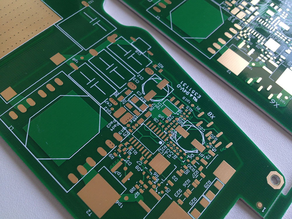
Why does this happen? Because designing a board that works once is fundamentally different from designing a board that can be manufactured efficiently at scale.
In this comprehensive guide, we will bridge the “Valley of Death” between prototyping and mass production. You will learn how to adapt your manufacturing strategies for different batch sizes, implement early Design for Manufacturing (DFM) rules, and avoid the hidden supply chain traps that derail product launches. Whether you are transitioning from 50 units to 5,000, or aiming for global distribution, this guide will serve as your roadmap.
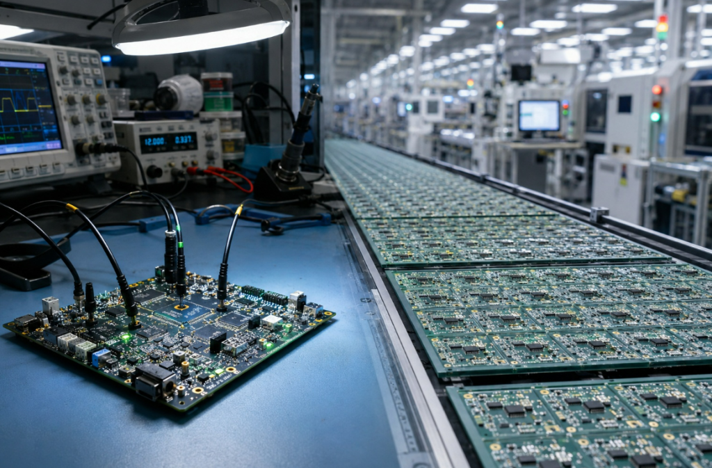
Understanding the PCB NPI Process: Why the Transition Fails
The transition from a prototype to mass production is rarely a simple copy-paste operation. In North American and European markets, hardware teams are highly risk-averse, and for good reason. A single design flaw that goes unnoticed in a batch of 10 boards can result in hundreds of thousands of dollars in scrapped materials when scaled to 10,000 boards.
The primary friction points during this New Product Introduction (NPI) phase include:
- Material Unavailability: Prototypes often use exotic or highly specific laminates that are available in small quantities but have 20-week lead times for bulk orders.
- Poor Panel Utilization: A board size that isn’t optimized for standard factory panel dimensions can result in up to 40% wasted FR4 material, driving up unit costs.
- Tolerance Stacking: Minor manufacturing variances that are acceptable in a single board compound in mass production, leading to mechanical fit issues or electrical failures.
To mitigate these risks, hardware teams must shift their mindset from “getting it to work” to “getting it to yield.” This requires partnering early with a reliable PCB manufacturing partner who can provide transparent cost-benefit analyses and strict DFM guidelines before the first pilot run is even ordered.
Core Concepts Simplified: Prototyping vs. Volume Production
To understand how to adapt your process, we need to strip away the complex jargon and look at the core concepts driving PCB manufacturing costs and reliability.
DFM (Design for Manufacturing) is like building a house foundation.
Designing a complex 12-layer PCB without mass-production rules in mind is exactly like building a 50-story skyscraper on a foundation meant for a garden shed. It might hold up the first floor (your prototype), but as you add scale and weight (mass production), the entire structure collapses under its own inconsistencies. Early DFM checks—such as adjusting annular rings, trace spacing, and drill sizes to match factory capabilities—save weeks of redesign time later.
Material Selection is like standardizing baking ingredients.
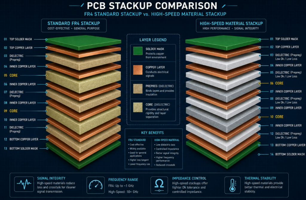
Imagine baking a cake for a competition using a rare, imported vanilla bean. It tastes amazing. Now, imagine you are asked to bake 10,000 of those cakes by next week. If you can’t buy that specific vanilla in bulk, your production line stops. In PCB manufacturing, the “ingredients” are your Core and Prepreg materials. Using standard Tg (Glass Transition Temperature) materials early ensures supply chain consistency when you scale up.
The Batch Size Comparison Matrix
Understanding the shifting priorities at different production volumes is critical for procurement and engineering alignment.
| Production Phase | Typical Batch Size | Primary Engineering Goal | Cost Driver | Key Strategy |
|---|---|---|---|---|
| Prototyping | 1 – 50 units | Functional verification, speed to market | NRE (Non-Recurring Engineering) setup fees | Use standard stackups; ignore panel waste temporarily. |
| Pilot Run (NPI) | 50 – 1,000 units | Process validation, yield testing | Material utilization, testing time | Implement strict DFM; finalize material standardization. |
| Mass Production | 10,000+ units | Cost optimization, extreme reliability | Scrap rate, panel waste, assembly fallout | Maximize panelization efficiency; automate testing (AOI/ICT). |
Step-by-Step Guide to Scaling Multilayer PCBs
Scaling successfully requires a methodical approach. Here is the actionable, step-by-step process that industry veterans use to transition designs without bleeding capital.
Step 1: Enforce DFM at the Schematic and Layout Stage
Do not wait until the layout is finished to talk to your fabricator. Request their standard stackup and design rule check (DRC) files before you route a single trace. Ensure your design complies with global standards like IPC-2221 (Generic Standard on Printed Board Design) and IPC-A-600 (Acceptability of Printed Boards). Designing to IPC Class 2 or Class 3 standards from day one eliminates the need for a major layout overhaul later.
Step 2: Standardize Impedance Control and Materials
Impedance control ensures that high-speed electrical signals travel smoothly through the PCB without bouncing back and causing data errors. Think of it like tuning a water pipe: if the pipe’s diameter changes suddenly, water pressure fluctuates, causing turbulence.
During prototyping, your fab might achieve your target 50-ohm impedance using a specific resin content. When moving to mass production at a different facility, they might use slightly different Prepreg brands. Always specify the target impedance in your fab notes, rather than rigid trace widths, allowing the manufacturer to adjust the geometry slightly to match their specific material properties. Validate this with TDR (Time-Domain Reflectometry) testing during the pilot run.
Step 3: Optimize Panelization and Material Utilization
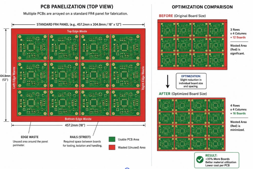
Panelization is the art of fitting your individual PCBs onto a large, standard manufacturing panel (e.g., 18″ x 24″). Think of it like cutting cookies from a sheet of dough. Your goal is to leave as little scrap dough as possible.
If your board is 105mm x 105mm, you might fit 12 boards on a panel with 35% waste. By reducing your board size by just 5mm (to 100mm x 100mm), you might suddenly fit 16 boards on that exact same panel, slashing your per-unit manufacturing cost instantly.
Batch Size Strategy & Specification Table
Use this specification matrix to adapt your engineering focus based on your current order volume:
| Specification Focus | 1-50 Units (Prototype) | 500-2,000 Units (Pilot) | 10,000+ Units (Mass Production) |
|---|---|---|---|
| Material Sourcing | Use whatever is in stock. | Lock in a single material brand (e.g., Shengyi, Isola). | Secure 6-month supply chain forecasts. |
| Panelization | Single boards or basic arrays. | Array optimized for SMT assembly lines. | Array optimized for maximum raw material yield (>80%). |
| Depanelization | Manual break-aways. | Tab routing with mouse bites. | V-scoring for automated separation. |
| Testing | Flying Probe Testing (slow, cheap setup). | Flying Probe / Bed of Nails transition. | Custom Bed of Nails / ICT (fast, expensive setup). |
Scenario A: Scaling Standard Multilayer Boards (4-12 Layers)
For standard digital boards, the transition is mostly about cost reduction. The focus here should be on standardizing drill sizes. Every unique via size requires a different drill bit and tool change in the CNC machine. Reducing your drill sizes from 15 unique diameters to just 4 standard diameters can shave hours off the manufacturing time of a large batch.
Scenario B: Scaling Complex HDI & Rigid-Flex Designs
When dealing with High-Density Interconnect (HDI) boards, the risks multiply. HDI relies on microvias—extremely tiny, laser-drilled holes used to connect different layers. While they save a massive amount of space in prototypes, microvias require highly precise manufacturing.
If you are scaling up, you must carefully evaluate your HDI PCB stackup. A 1+N+1 structure is relatively easy to mass-produce, but moving to an Any-Layer HDI structure increases the risk of microvia failure during thermal cycling at scale. Similarly, if your product folds or bends, strictly adhering to rigid-flex PCB design guidelines during the NPI phase is non-negotiable to prevent trace fracturing after thousands of bending cycles in the field.
Expert Tips & Common Pitfalls to Avoid
If you spend time on engineering forums like r/PrintedCircuitBoard or EEVblog, you will see the same scale-up horror stories repeated constantly. Here are the most common pitfalls and how to avoid them based on real-world NPI experience.
Pitfall 1: Ignoring Microvia Reliability in Thermal Cycling
The Mistake: Stacking microvias directly on top of each other across 4 or more layers in a prototype, then pushing it to mass production.
The Reality: During the reflow soldering process, the PCB expands. Stacked microvias experience immense Z-axis stress. In a batch of 10 prototypes, they might survive. In a batch of 10,000, 5% of your boards might suffer from hidden microvia cracking, leading to intermittent field failures that are a nightmare to debug.
The Fix: Stagger your microvias unless absolutely necessary. If you are dealing with extreme complexity, such as an ultra-high layer count PCB, work with a manufacturer that conducts rigorous interconnect stress testing (IST).
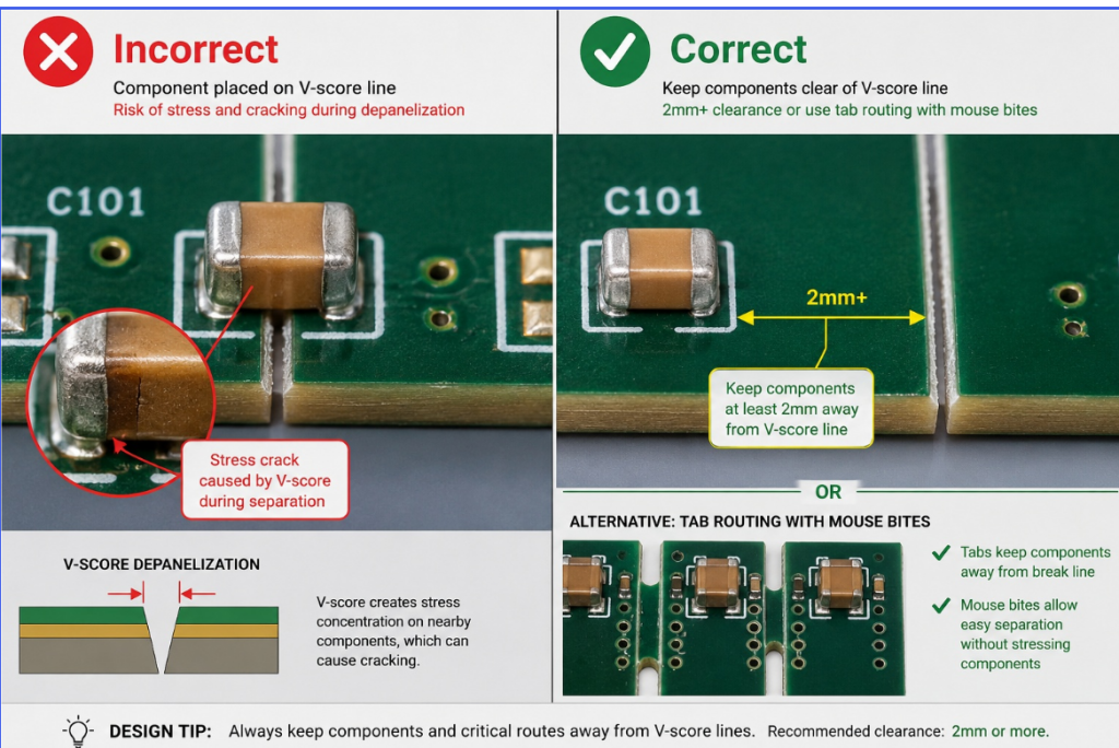
Pitfall 2: The V-Scoring vs. Tab Routing Trap
The Mistake: Choosing the wrong depanelization method for assembled boards.
The Reality: V-scoring cuts a V-shaped groove for easy snapping, which is incredibly fast for mass production. However, if you place sensitive ceramic capacitors (MLCCs) too close to the V-score line, the mechanical stress of snapping the boards apart will crack the capacitors. Tab routing (using small bridges with mouse bites) is safer for components near the edge but leaves rough edges and takes longer to route.
The Fix: Keep all components at least 2mm away from V-score lines. Use tab routing for oddly shaped boards, and V-scoring for straight, rectangular mass-production panels.
Pitfall 3: Over-Constraining Tolerances
Engineers often apply extreme tolerances (e.g., +/- 5% on impedance, or ultra-tight drill registrations) “just to be safe.” In mass production, tighter tolerances mean lower factory yields. If the factory has to scrap 20% of the boards just to meet an unnecessarily tight tolerance, they will pass that cost directly to you. Only specify tight tolerances where the electrical or mechanical design absolutely demands it.
Conclusion & Final Thoughts
Transitioning a multilayer PCB from a lab prototype to a mass-produced commodity is one of the most challenging phases of hardware development. It requires a shift from purely electrical engineering to mechanical, chemical, and supply chain management.
By implementing DFM early, understanding the cost implications of material utilization, and avoiding common structural pitfalls like stacked microvia failures, you can navigate the NPI process smoothly. Remember, the goal is not just to build a board that works, but to build a board that yields a 99% pass rate on the assembly line.
Quick Summary: Prototype to Mass Production Checklist
| Category | Key Action Item | Why it Matters |
|---|---|---|
| Design (DFM) | Run factory-specific DRCs before routing. | Prevents costly layout redesigns. |
| Materials | Specify target impedance, not just trace width. | Allows factories to match available materials. |
| Cost Control | Adjust board dimensions to maximize panel yield. | Can reduce unit costs by up to 30%. |
| Reliability | Stagger microvias; keep parts away from V-scores. | Prevents thermal cycling and mechanical failures. |
If you are preparing for an NPI pilot run and need a thorough DFM review to ensure your design is ready for scale, partnering with the right fabricator is your best insurance policy. Start optimizing your stackup today to guarantee a flawless mass production launch tomorrow.
Frequently Asked Questions
Q1: What is the main difference between PCB prototyping and mass production?
A: Prototyping prioritizes speed and functional verification using small batches. Mass production focuses on DFM compliance, material standardization, panelization efficiency, and yield optimization to minimize per-unit costs.
Q2: What is DFM and why does it matter for scaling?
A: Design for Manufacturing (DFM) ensures your layout aligns with factory capabilities. Implementing DFM early prevents costly redesigns, improves yield rates, and avoids tolerance stacking issues at scale.
Q3: How can I reduce costs when scaling to mass production?
A: Optimize board dimensions for panel utilization, standardize drill sizes to reduce CNC tool changes, and avoid over-constraining tolerances beyond what the electrical design actually requires.
Q4: Why are stacked microvias risky in high-volume production?
A: Stacked microvias experience extreme Z-axis thermal stress during reflow. What works in 10 prototypes can cause hidden cracking in 5% of a 10,000-unit batch. Always stagger microvias when possible.
Q5: Should I use V-scoring or tab routing for depanelization?
A: Use V-scoring for straight, rectangular panels in high-volume runs. Use tab routing for odd-shaped boards or when sensitive components must be placed near the board edge.