Advantages and Disadvantages of HDI PCB Design: A Complete Guide for 2026
High Density Interconnect (HDI) PCB technology has transformed modern electronics manufacturing, enabling devices to become smaller, faster, and more powerful. But is HDI the right choice for your project? This guide explores the complete picture—from space-saving benefits to cost considerations—helping you make an informed decision.
What is HDI PCB Technology?
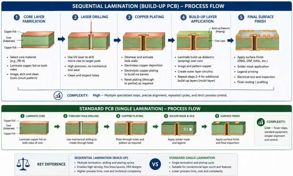
HDI (High Density Interconnect) PCB represents an advanced circuit board manufacturing approach that uses laser-drilled microvias, fine-line traces, and sequential lamination to achieve significantly higher component density than conventional PCBs.
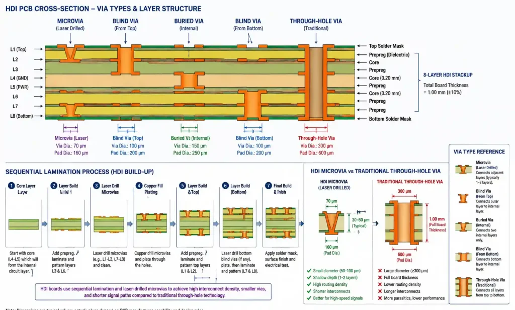
According to IPC-2226 standards, HDI PCBs are characterized by:
- Microvias: Diameter ≤150μm (0.15mm), compared to ≥300μm for standard vias
- Fine line traces: Width and spacing ≤100μm (some manufacturers achieve 75μm or less)
- Connection density: ≥20 pads per cm²
- Capture pads: ≤400μm diameter
Unlike traditional through-hole vias that penetrate the entire board, HDI uses blind vias (connecting outer to inner layers) and buried vias (connecting inner layers only). This creates routing flexibility impossible with standard PCB technology.
Key Long-Tail Keywords: What is HDI PCB, high density interconnect meaning, HDI board definition, microvia PCB technology, laser drilled PCB
Key Advantages of HDI PCB Design
Superior Miniaturization and Space Efficiency
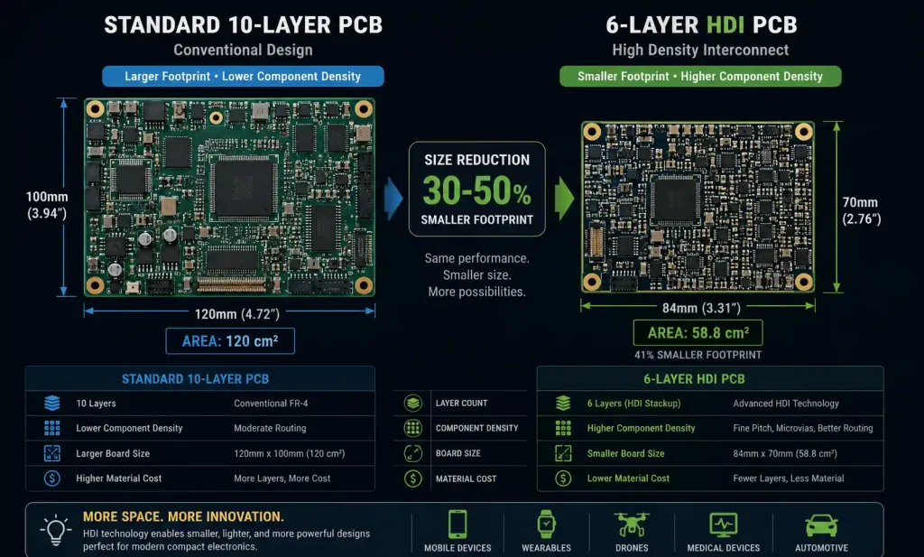
HDI technology achieves 30-50% smaller board sizes compared to standard PCBs with equivalent functionality. This dramatic size reduction comes from:
- 4x higher routing density per unit area
- Elimination of oversized through-holes that waste board space
- Ability to place vias directly in component pads (via-in-pad technology)
- Stacked and staggered microvia configurations
For modern smartphones containing 8-12 layer HDI boards, this space efficiency is the difference between fitting all components or requiring a larger device footprint.
Enhanced Electrical Performance
HDI boards deliver measurable performance improvements:
Signal Integrity: Shorter signal paths reduce propagation delay and signal loss. Microvias create vertical transitions of just 50-100μm compared to 1-2mm for traditional vias, minimizing via stubs that cause signal reflections.
Impedance Control: Tighter manufacturing tolerances (±10% vs ±15-20% for standard PCBs) enable more predictable impedance matching for high-speed signals.
Power Distribution: HDI’s layer structure allows dedicated power and ground planes positioned closer to signal layers, reducing power supply noise and electromagnetic interference (EMI).
Crosstalk Reduction: Higher density doesn’t mean more noise—proper HDI design with microvias and appropriate spacing actually reduces crosstalk compared to cramped standard PCB layouts.
Advanced Component Support
HDI technology enables use of cutting-edge components:
- Fine-pitch BGAs: Support for components with pitch down to 0.4mm (0.2mm experimental)
- Package miniaturization: 0201 (0.6mm × 0.3mm) and smaller chip components
- High pin-count devices: Escape routing for 500+ pin BGAs where standard vias cannot fit between pads
Reduced Layer Count Potential
Counterintuitively, HDI’s higher routing density can reduce total layer count in complex designs. A 10-layer standard PCB might be achievable in 6-8 HDI layers, potentially offsetting some of HDI’s cost premium while reducing board thickness and weight.
Improved Reliability
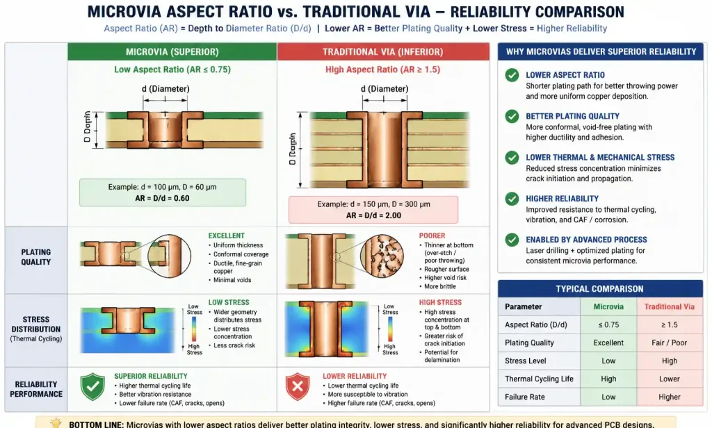
Despite smaller features, HDI boards maintain excellent reliability:
- Laser-drilled microvias have better aspect ratios (depth:diameter) than mechanically drilled holes
- Sequential lamination creates stronger layer-to-layer bonds
- Reduced thermal stress from smaller vias and better heat distribution
Better Thermal Management
Microvias function as thermal conductors between layers, creating more heat dissipation pathways. Combined with HDI’s compact design, this enables effective thermal management in power-dense applications like AI accelerators and 5G modules.
Key Long-Tail Keywords: HDI PCB benefits, advantages of high density PCB, why use HDI boards, HDI vs standard PCB performance, microvia benefits
Major Disadvantages and Challenges
Significantly Higher Manufacturing Costs
The most substantial drawback: HDI boards cost 2.3-3.2× more than comparable standard PCBs.
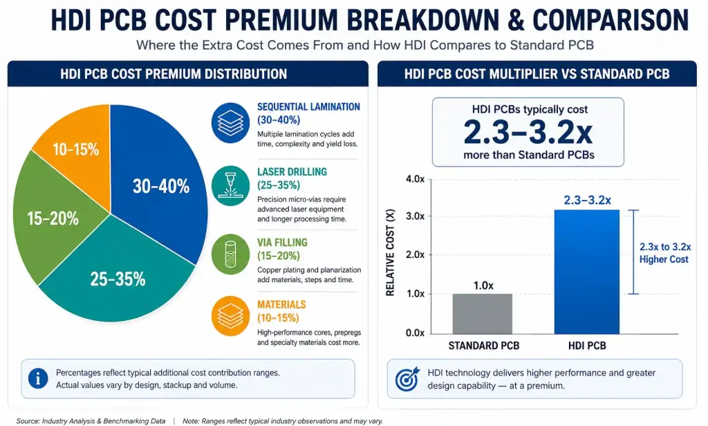
This premium stems from:
- Sequential lamination cycles: Each build-up layer requires separate lamination, adding process steps
- Laser drilling setup: Equipment costs and per-hole drilling time exceed mechanical drilling
- Via filling requirements: Microvias often require conductive or non-conductive filling before subsequent layers
- Yield considerations: Tighter tolerances mean higher rejection rates
For prototypes or low-volume production (under 100 units), this cost difference can be prohibitive. Even at higher volumes, the 2-3× cost multiplier requires strong justification through performance gains or miniaturization necessity.
Increased Design Complexity
HDI design demands more expertise and time:
- Layer stackup planning: Sequential build-up requires careful planning of via placement and layer transitions
- Thermal management: Higher component density concentrates heat, requiring detailed thermal analysis
- Impedance discontinuities: Microvia transitions can create impedance mismatches in high-speed designs
- Design rule constraints: Must align with manufacturer capabilities (via sizes, spacing, aspect ratios)
Design cycles typically increase 20-30% compared to standard PCB projects of similar complexity.
Manufacturing Risk and Lead Time
HDI’s complexity introduces risks:
- Higher layout error risk: Dense routing increases chances of short circuits, insufficient trace width, or signal integrity issues
- Limited manufacturer base: Not all PCB fabricators offer HDI capabilities, reducing sourcing options
- Longer lead times: Sequential lamination and laser drilling extend production cycles by 1-2 weeks
- Rework challenges: Repairing HDI boards requires specialized equipment and is often impractical
A design error discovered after fabrication can trigger costly layout revisions and delays, potentially pushing EVT (Engineering Verification Test) schedules.
Testing and Inspection Challenges
Quality assurance becomes more difficult:
- Electrical testing: Buried vias and microvias are harder to probe for testing
- X-ray inspection: Required for hidden via structures, adding inspection time and cost
- Defect detection: Smaller features make visual inspection less effective
Limited DIY and Prototyping Options
For hobbyists, startups, or rapid prototyping:
- Few PCB fabricators offer affordable HDI prototyping services
- Minimum order quantities often higher than standard PCBs
- Design tool capabilities may be insufficient without premium CAD software
Supply Chain Considerations
HDI’s specialized nature affects supply chains:
- Vendor lock-in risk: Switching fabricators may require design modifications
- Capability variations: What’s “standard HDI” for one manufacturer may be advanced for another
- Material availability: Specialized thin dielectrics and copper foils may have longer lead times
Key Long-Tail Keywords: HDI PCB disadvantages, high density PCB challenges, HDI board limitations, HDI manufacturing problems, cost of HDI PCB
HDI vs Standard PCB: When to Choose HDI
Decision Matrix
| Factor | Choose HDI When… | Choose Standard PCB When… |
|---|---|---|
| Space | Size/weight critical | Space not constrained |
| Component Density | Fine-pitch BGAs, high pin counts | Standard components (≥0.5mm pitch) |
| Signal Frequency | >1 GHz signals, DDR4/5 memory | Lower frequency (<500 MHz) |
| Production Volume | >1,000 units (cost amortization) | Prototypes, low volume (<500 units) |
| Budget | Performance justifies 2-3× cost | Cost-sensitive applications |
| Development Timeline | Schedule accommodates complexity | Fast time-to-market critical |
| Layer Count | Can reduce layers vs standard approach | Routing achievable in standard layers |
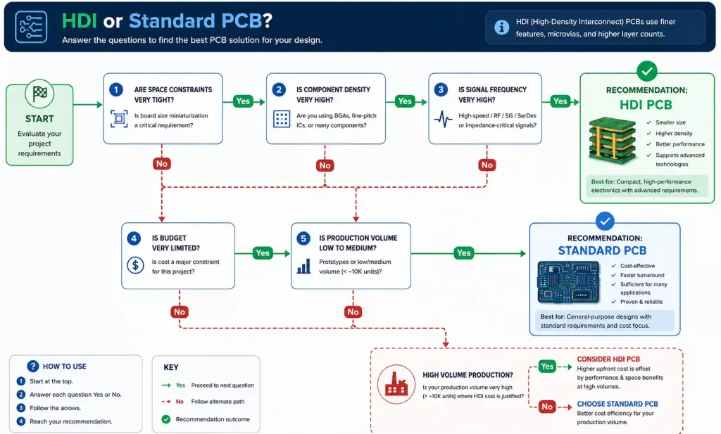
When HDI is Essential
- Smartphones and wearables: Size constraints make HDI non-negotiable
- Medical implantables: Miniaturization and reliability requirements
- High-speed digital: DDR5, PCIe 5.0, 100G+ networking
- Advanced AI/ML hardware: Thermal and density demands
- Aerospace/defense: Weight reduction critical
When Standard PCB is Sufficient
- Industrial controls: Durability and cost matter more than size
- Consumer electronics (non-portable): Space available for standard approach
- Power electronics: Focus on thermal and current handling, not density
- Prototyping phase: Validate concept before committing to HDI
Key Long-Tail Keywords: HDI PCB vs standard PCB, when to use HDI, HDI or traditional PCB, choosing PCB technology, HDI application guide
Real-World Applications of HDI PCBs
Consumer Electronics (45% of HDI Market)
- Smartphones: Flagship devices use 8-12 layer HDI with any-layer vias
- Tablets and laptops: Main boards transitioning from standard to HDI
- Wearables: Smartwatches, fitness trackers demand ultra-compact HDI
- True wireless earbuds: Some of the smallest HDI implementations
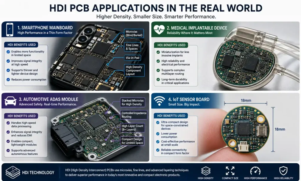
Medical Devices (18% of HDI Market)
- Implantable devices: Pacemakers, neurostimulators, cochlear implants
- Diagnostic equipment: Portable ultrasound, handheld analyzers
- Surgical instruments: Minimally invasive tools with embedded electronics
- Continuous monitoring: Glucose sensors, cardiac monitors
Automotive Electronics (12% of HDI Market)
- ADAS systems: Camera modules, radar, LiDAR processing
- Infotainment: High-resolution displays, connectivity modules
- EV battery management: Space-constrained power electronics
- Autonomous driving: High-performance computing platforms
Industrial and IoT (25% of HDI Market)
- 5G infrastructure: Small cell base stations, mmWave modules
- Edge computing: Compact AI inference devices
- Industrial IoT sensors: Battery-powered long-range sensors
- Drones and robotics: Weight-sensitive embedded systems
Key Long-Tail Keywords: HDI PCB applications, where HDI is used, HDI in smartphones, medical device HDI, automotive HDI PCB
Cost Considerations and ROI Analysis
Understanding HDI Cost Structure
Per-Unit Cost Breakdown:
- Sequential lamination cycles: 30-40% of premium
- Laser drilling: 25-35% of premium
- Via filling and plating: 15-20% of premium
- Materials (thin dielectrics): 10-15% of premium
Cost Mitigation Strategies
- Optimize layer count: Every HDI build-up layer adds cost—minimize sequential layers
- Strategic microvia placement: Use microvias only where necessary, standard vias elsewhere
- Panel utilization: Optimize board dimensions for better panel array efficiency
- Volume commitment: Negotiate pricing for annual volume commitments
- Design for manufacturing: Work with fabricator during design phase to avoid costly features
ROI Scenarios Where HDI Pays Off
Scenario 1: Size-Driven Products
- Product: Consumer wearable
- Standard PCB approach: 35mm × 25mm × 1.6mm (10 layers)
- HDI approach: 28mm × 20mm × 0.8mm (6 layers HDI)
- Result: 36% volume reduction enables smaller case, better aesthetics—justifies 2.5× PCB cost
Scenario 2: Layer Count Reduction
- Product: High-speed data acquisition
- Standard PCB approach: 12 layers, $45 per board
- HDI approach: 8 layers HDI, $95 per board
- Result: At 5,000 units, thinner profile enables $8 savings on enclosure—net savings $3 per unit
Scenario 3: Performance Critical
- Product: 5G mmWave module
- Standard PCB approach: Cannot meet signal integrity requirements
- HDI approach: Only viable solution
- Result: HDI cost irrelevant—it’s a technical necessity
Key Long-Tail Keywords: HDI PCB cost, HDI pricing guide, HDI cost analysis, HDI ROI calculation, expensive HDI PCB
Future Trends in HDI Technology
Market Growth Trajectory
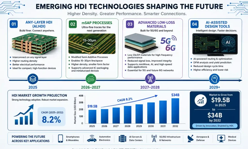
The global HDI PCB market is projected to grow from USD 19.5 billion in 2025 to over USD 34 billion by 2032, representing a CAGR of 8.3%. This growth reflects HDI’s transition from specialty technology to mainstream requirement in consumer electronics.
Emerging Technical Trends
1. Any-Layer HDI (ALHDI)
Moving beyond stacked and staggered microvias to any-layer interconnection, enabling ultimate routing flexibility. Already in flagship smartphones, expanding to other applications.
2. mSAP (Modified Semi-Additive Process)
Enabling trace widths down to 15-30μm (compared to 50-75μm typical today), supporting even higher density and finer-pitch components.
3. Advanced Materials
- Low-loss dielectrics for 5G/6G millimeter-wave applications
- Thermally conductive dielectrics for improved heat dissipation
- Flexible and rigid-flex HDI for wearables
4. Integration with Package Substrates
Blurring lines between HDI PCBs and IC substrates, enabling system-in-package (SiP) approaches with HDI as the foundation.
5. AI-Assisted Design Tools
Machine learning optimizing HDI routing, via placement, and thermal management—reducing design time and improving manufacturability.
Sustainability Initiatives
- Material reduction: Thinner boards and fewer layers reduce copper and laminate usage
- Recycling advances: Improved processes for recovering materials from complex HDI structures
- Energy efficiency: Smaller devices consume less operational energy over lifetime
Key Long-Tail Keywords: HDI PCB trends 2026, future of HDI technology, any-layer HDI, advanced HDI PCB, next generation PCB
Best Practices for HDI PCB Design
Design Guidelines
Via Management
- Use microvias for high-density areas, standard vias where possible
- Avoid stacking more than 2 microvias without staggering (reliability concern)
- Maintain minimum 100μm spacing between microvia edges
- Fill vias when stacking or placing components above
Trace Routing
- Minimum 75μm trace width/spacing for manufacturability (50μm possible but costly)
- Maintain consistent impedance on high-speed signals through microvia transitions
- Use reference planes adjacent to signal layers for controlled impedance
Thermal Management
- Create thermal vias arrays under power components
- Consider copper thickness distribution across layers
- Perform thermal simulation early in design process
Stackup Planning
- Work with fabricator to define achievable stackup before layout
- Place high-speed signals on layers with best impedance control
- Balance copper distribution to prevent warpage
Choosing an HDI Fabricator
Look for manufacturers offering:
- Clear capability documentation (via sizes, aspect ratios, line widths)
- DFM (Design for Manufacturing) review services
- Quality certifications (IPC Class 2 minimum, Class 3 for medical/aerospace)
- Reference designs or design guides specific to their process
Key Long-Tail Keywords: HDI PCB design guide, HDI design best practices, HDI layout tips, HDI design rules, designing HDI boards
Conclusion: Is HDI Right for Your Project?
HDI PCB technology offers compelling advantages—dramatic miniaturization, enhanced performance, and support for advanced components—but comes with significant cost premiums and design complexity.
Choose HDI when:
- Physical size/weight constraints demand it
- Component density exceeds standard PCB capabilities
- Signal integrity requirements exceed standard PCB performance
- Production volumes justify the cost differential
- Your product’s value proposition depends on compact form factor
Stick with standard PCBs when:
- Space is available for conventional routing
- Budget constraints are paramount
- Development timeline is aggressive
- Production volume is low (<500-1,000 units)
- Component technology doesn’t require HDI features
The HDI vs standard decision isn’t about which technology is “better”—it’s about matching technology to requirements. As HDI costs decrease and capabilities expand, it’s becoming the default for more applications. But for many projects, standard PCB technology remains the practical, cost-effective choice.
Making Your Decision: Start by listing your absolute requirements (size, performance, cost, timeline). If size or electrical performance pushes the boundaries of standard PCB, explore HDI with your fabrication partner. Get quotes for both approaches with realistic volumes. Factor in the total product cost, not just PCB cost—sometimes a 3× PCB premium is offset by savings elsewhere in the system.
FAQ: Common Questions About HDI PCB Design
Q: Can any PCB manufacturer make HDI boards?
No. HDI requires laser drilling equipment, sequential lamination capabilities, and process expertise. Verify your fabricator’s specific HDI capabilities before designing.
Q: How much more expensive is HDI really?
Expect 2.3-3.2× cost premium for comparable designs. The gap narrows at higher volumes (>5,000 units) and with simpler HDI configurations (1+N+1 stackups).
Q: Is HDI more reliable than standard PCB?
When properly designed and manufactured, HDI offers equivalent or better reliability. The smaller vias actually have better aspect ratios, and sequential lamination creates strong layer bonds.
Q: What’s the minimum volume to justify HDI?
Generally 1,000-2,000 units for cost-sensitive applications, but lower if technical requirements mandate HDI or if size enables system-level savings.
Q: Can I prototype with HDI?
Yes, but expect higher costs ($200-500+ for prototypes vs $50-150 for standard PCB) and longer lead times (3-4 weeks vs 1-2 weeks). Some fabricators offer “quick-turn HDI” services.