HDI PCB Evolution: From 1st Gen to ELIC Technology
High-Density Interconnect (HDI) PCBs have transformed how we approach circuit board design over the past two decades. In our manufacturing facility, we’ve witnessed the transition from basic microvia designs to sophisticated any-layer interconnection structures. This evolution wasn’t just about smaller features—it fundamentally changed what’s possible in electronics miniaturization. Let’s explore how HDI technology progressed from simple single-layer microvia boards to today’s advanced ELIC (Every Layer Interconnection) architectures.
Table of Contents
- What Makes HDI Different from Standard PCBs
- First Generation HDI: The Foundation
- Second Generation: Staggered Microvias
- Third Generation: Stacked Microvias
- Advanced HDI: Any-Layer Technology
- ELIC Technology: The Current Frontier
- Comparing HDI Generations
- Choosing the Right HDI Generation
1. What Makes HDI Different from Standard PCBs
HDI technology centers on microvia structures—laser-drilled holes typically under 150 microns in diameter. Unlike traditional PCBs that rely on through-holes connecting all layers, HDI uses blind and buried vias to create connections exactly where needed. In our production runs for smartphone manufacturers, we regularly work with trace widths down to 50 microns and spaces at 50 microns, compared to the 150/150 standard for conventional boards.
The density advantage is measurable. A typical 10-layer HDI board can match or exceed the routing capacity of a 20-layer conventional PCB while being thinner and lighter. We’ve replaced 16-layer standard builds with 10-layer HDI designs for automotive radar modules, cutting the final thickness from 2.4mm to 1.6mm without compromising functionality.
2. First Generation HDI: The Foundation
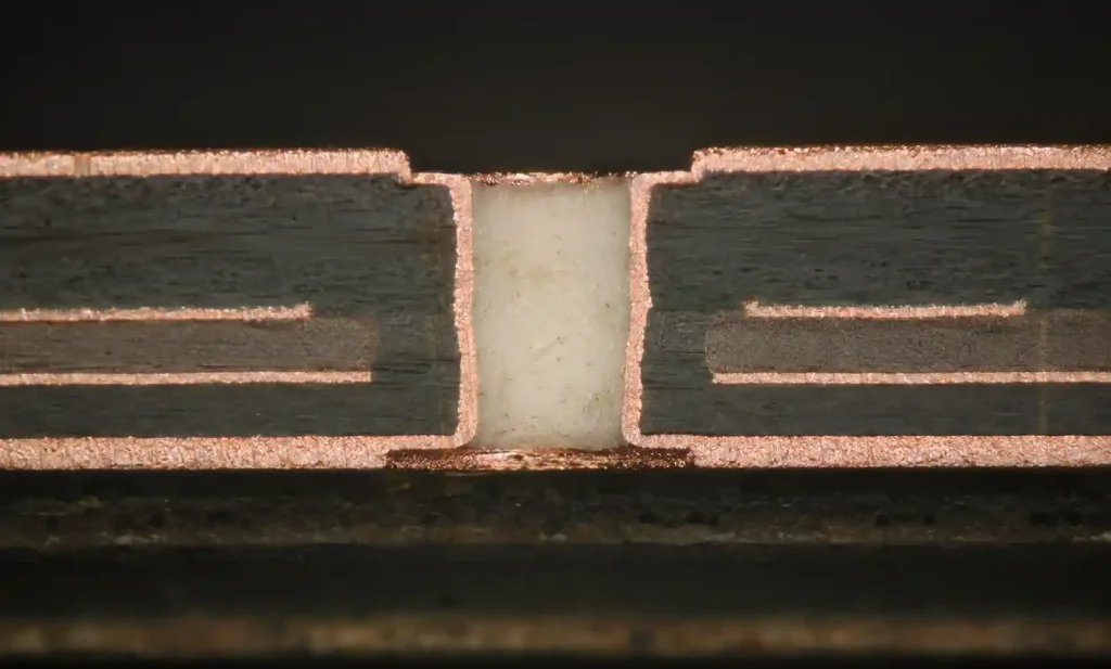
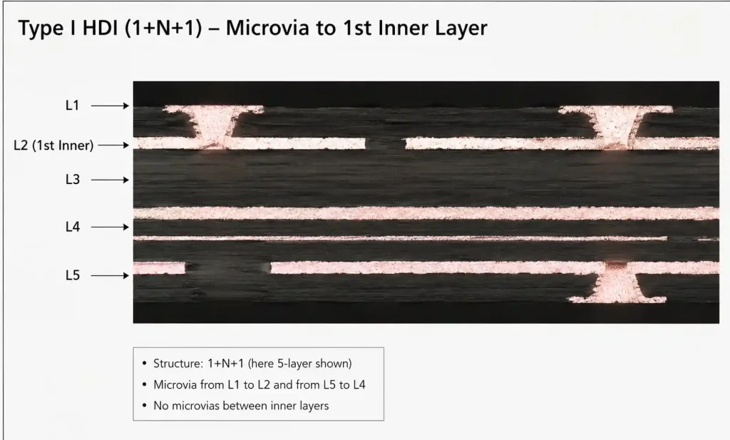
First-generation HDI (1+N+1) features a single layer of microvias on each outer surface, connecting to the first inner layer. The core remains a traditional multilayer stackup with through-holes. This architecture emerged in the late 1990s when mobile phones first demanded higher component density than conventional PCBs could deliver.
From a manufacturing perspective, Type I HDI boards are the most accessible entry point. We use CO2 lasers for microvia drilling, achieving diameters between 100-150 microns. The key limitation: you can only escape one ring of BGA pads through the outer layer microvias. For a 0.5mm pitch BGA, this means the outer rows route through microvias while inner pads still require buried vias or complex routing.
Common applications we see:
- Consumer electronics with moderate density requirements
- Industrial controls transitioning from conventional PCB
- Cost-sensitive smartphone peripherals
- Wearable device main boards
The manufacturing yield for Type I HDI typically runs 5-8% higher than more advanced types, which explains why many mid-range products stay at this level when density permits.
3. Second Generation: Staggered Microvias
Second-generation HDI (2+N+2) adds microvia layers on both sides but staggers them—microvias on one layer don’t directly stack on those below. This allows routing through two BGA pad rows from each surface. In our experience with networking equipment, Type II structures handle BGAs up to 0.4mm pitch more efficiently than Type I without the yield risks of stacked vias.
The staggered approach provides a middle ground. You gain significant density improvement over Type I while maintaining relatively straightforward manufacturing. However, the design requires careful planning—since vias can’t stack, you must map escape routing layer by layer to avoid congestion. We typically see 10-15% more design time for Type II versus Type I layouts.
Manufacturing considerations:
- Sequential lamination cycles (typically 2-3 cycles)
- Laser drilling after each lamination
- Via filling required for surface planarity
- More complex impedance control due to varied stackup zones
Type II HDI suits applications where component density matters but cost constraints limit going to fully stacked structures. We produce significant volumes for automotive infotainment systems and mid-tier smartphones at this level.
4. Third Generation: Stacked Microvias
Third-generation HDI (3+N+3 or higher) allows microvias to stack directly on top of each other, creating vertical interconnection channels through multiple layers. This architecture enables routing through three or more BGA pad rows per side, essential for fine-pitch components below 0.4mm. In our facility, stacked via designs represent about 35% of our HDI production, primarily for flagship smartphones and high-end computing.
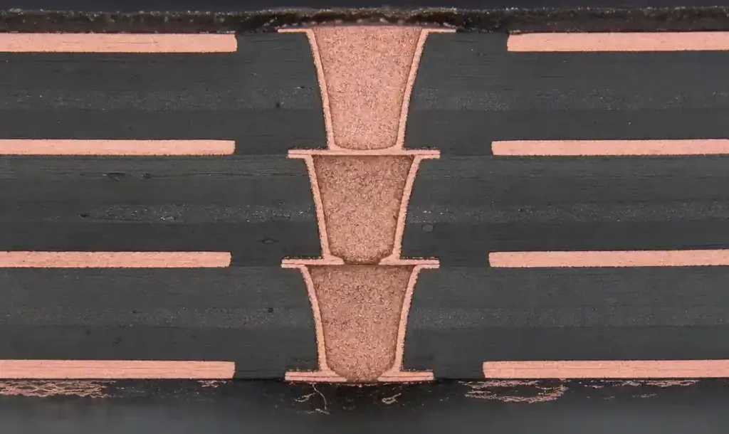
The stacking capability solves a critical problem: escaping fine-pitch BGAs without consuming excessive routing layers. A 0.35mm pitch BGA with 20×20 pads can be completely escaped using stacked microvias, where Type II would require additional routing layers or impossible trace geometry. However, stacked vias introduce manufacturing complexity. Each via must land precisely on the one below—we hold positional tolerance to ±50 microns across the entire panel.
Key manufacturing challenges:
- Aspect ratio control (depth-to-diameter typically ≤1:1 for reliable filling)
- Via filling quality (voids cause reliability failures)
- Registration accuracy between lamination cycles
- Copper plating uniformity in stacked structures
We’ve found that Type III yields run 8-12% lower than Type II in initial production, though mature processes narrow this gap. The cost premium is 40-60% over Type II HDI, justifiable when board space savings eliminate layers or enable smaller form factors.
5. Advanced HDI: Any-Layer Technology
Any-layer HDI represents a shift from sequential buildup to structures where microvias can connect any layer to any other layer within the stackup. Unlike Type III that builds from outside in, any-layer technology (sometimes called Type IV or Type V) uses staggered and stacked vias throughout the entire board thickness to create three-dimensional routing networks.
In our production for high-performance computing modules, any-layer designs let us place components on both sides with equal routing access to all internal planes. This matters for applications like AI accelerators where dozens of high-speed differential pairs must route between processors, memory, and power delivery networks without layer-count explosion.
The design freedom comes at a cost. Any-layer boards require sophisticated simulation—signal integrity, power integrity, and thermal modeling become essential rather than optional. We’ve seen designs where via placement affects impedance by ±5 ohms, enough to cause SI failures at multi-gigabit speeds. Layer count doesn’t tell the whole story anymore; via architecture determines performance.
Typical applications:
- Server processors with 2000+ BGA connections
- Network switches handling 400G+ data rates
- Advanced driver assistance systems (ADAS) with sensor fusion
- 5G infrastructure equipment
Manufacturing yields for any-layer HDI depend heavily on design quality. Well-designed boards achieve 75-80% yield; poorly optimized designs drop below 60%, making them economically unviable.
6. ELIC Technology: The Current Frontier
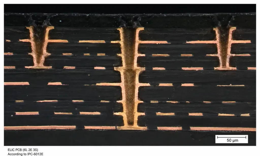
ELIC (Every Layer Interconnection Capable) technology represents the current peak of HDI evolution. The term comes from Japanese manufacturers who pioneered this approach for mobile devices requiring maximum functionality in minimum space. ELIC boards feature microvias that can span multiple layers in a single laser drilling operation, combined with any-layer interconnection capability.
What distinguishes ELIC from earlier any-layer designs is the process integration. We use conformal via filling methods that allow reliable stacking to three or four microvia levels, compared to the two-level limit in conventional Type III HDI. This enables routing density that previously required coreless substrates or IC packaging technologies.
In our recent project for a flagship smartphone camera module, ELIC technology allowed us to integrate image sensor, ISP, power management, and RF front-end onto a single 0.8mm thick board. The equivalent conventional HDI design would have required two separate boards or a package-on-package approach, both adding thickness and cost.
ELIC manufacturing requirements:
- Modified dielectric materials with improved laser drill quality
- Advanced via fill processes (copper paste or electroless plating)
- Micro-sections and X-ray inspection for every batch
- Design rules typically at 30/30 micron trace/space or finer
The economics of ELIC currently limit it to high-value applications. We’re seeing adoption in premium smartphones, professional cameras, advanced medical devices, and aerospace systems where performance justifies the 2-3x cost premium over standard Type III HDI.
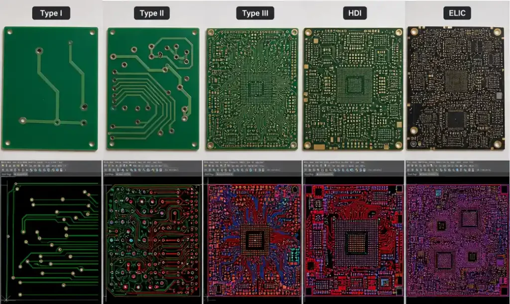
7. Comparing HDI Generations
| HDI Generation | Via Architecture | Max BGA Pitch Handled | Typical Layer Count | Relative Cost | Common Applications |
|---|---|---|---|---|---|
| Type I (1+N+1) | Single microvia layer per side | 0.5mm+ | 8-12 layers | 1.0x baseline | Consumer electronics, industrial controls, automotive peripherals |
| Type II (2+N+2) | Staggered microvias, 2 layers per side | 0.4-0.5mm | 10-14 layers | 1.3-1.5x | Mid-range smartphones, networking equipment, automotive infotainment |
| Type III (3+N+3+) | Stacked microvias, 3+ layers per side | 0.35-0.4mm | 12-18 layers | 1.6-2.0x | Flagship smartphones, tablets, high-end computing |
| Any-Layer | Microvias throughout stackup | 0.3-0.35mm | 14-24+ layers | 2.0-2.5x | Servers, network switches, ADAS, 5G infrastructure |
| ELIC | Multi-span microvias, any-layer | 0.25-0.3mm | 10-20 layers | 2.5-3.0x | Premium smartphones, professional cameras, medical devices, aerospace |
The technology progression isn’t just about smaller features—each generation enables different product architectures. Type I suits designs where component placement can be optimized around routing constraints. Type II and III enable dense component placement that drives board size reduction. Any-layer and ELIC technologies support ultra-high-speed signals and complex functionality integration that would otherwise require multiple boards or package-level solutions.
8. Choosing the Right HDI Generation
| Selection Factor | Type I/II Recommended | Type III Recommended | Any-Layer/ELIC Recommended |
|---|---|---|---|
| BGA pitch | ≥0.4mm | 0.35-0.4mm | ≤0.35mm |
| Signal speed | <10 Gbps | 10-25 Gbps | >25 Gbps |
| Board thickness target | >1.6mm | 1.0-1.6mm | <1.0mm |
| Component density | Moderate | High | Very high |
| Production volume | >10K units/year | >5K units/year | High-value regardless of volume |
| Budget constraint | Cost-sensitive | Performance-driven | Performance-critical |
The decision framework we use with clients starts with the component pitch of the finest BGA in the design. For 0.4mm and above, Type II usually provides the best cost-performance balance unless board space is severely constrained. Between 0.35-0.4mm, Type III becomes necessary for reliable escape routing. Below 0.35mm pitch, you’re typically looking at any-layer or ELIC technology.Signal integrity requirements often force the technology choice regardless of density. When we design boards with 56G PAM4 signals for data center applications, any-layer via architecture is essential to maintain controlled impedance and minimize stub lengths. The tighter via routing tolerance and ability to place vias precisely on the signal path outweighs the cost consideration.
Manufacturing ecosystem availability matters too. Type I and II HDI are widely available from numerous manufacturers globally. Type III narrows the supplier base significantly, while ELIC currently limits you to a handful of advanced manufacturers primarily in Asia. For products requiring multi-source manufacturing strategies, this reality may dictate settling for a less advanced HDI type even if the design could benefit from higher technology.
Project timeline also influences the decision. Type I HDI designs typically require 8-10 weeks from finalization to first articles. Type III extends this to 10-12 weeks, while ELIC can require 12-14 weeks due to the additional process validation and inspection requirements. If time-to-market is critical, a less advanced HDI type with proven manufacturing flow may outweigh the technical advantages of cutting-edge technology.
From our experience, about 60% of HDI designs could move down one technology generation with thoughtful component selection and placement optimization, reducing costs by 20-40% without compromising functionality. The remaining 40% genuinely require the advanced technology for reasons of physics—signal integrity, thermal management, or dimensional constraints that can’t be designed around.