BeO PCB Safety Considerations: Handling and Applications of Beryllium Oxide Circuit Boards
Beryllium oxide (BeO) PCBs offer exceptional thermal conductivity for high-power applications, but their unique material properties require strict safety protocols throughout design, manufacturing, and end-of-life disposal. This guide explains the critical safety considerations, handling requirements, and application scenarios where BeO substrates deliver performance advantages while maintaining workplace safety compliance.
Table of Contents
- Understanding BeO Material Properties and Safety Risks
- Critical Safety Protocols for BeO PCB Handling
- Design Guidelines for BeO Substrate Applications
- Manufacturing Process Safety Requirements
- Application Scenarios Where BeO PCBs Excel
- Alternative Materials Comparison
- FAQ
- Conclusion and Safety Compliance Recommendations
1. Understanding BeO Material Properties and Safety Risks
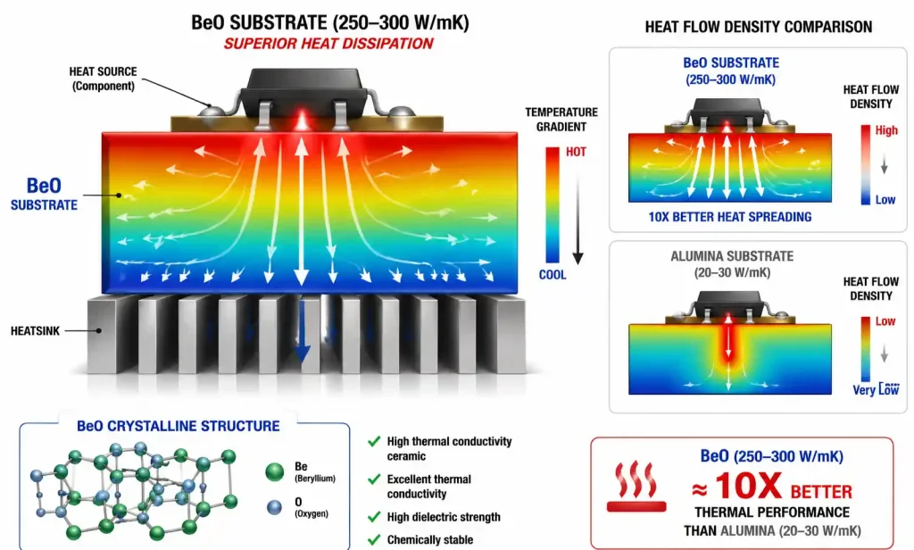
Beryllium oxide ceramic substrates provide thermal conductivity of 250-300 W/mK, approximately 10 times higher than standard alumina (Al₂O₃) substrates. This exceptional heat dissipation capability makes BeO attractive for RF power amplifiers, laser diode arrays, and high-voltage power modules operating above 150°C junction temperatures.
The primary safety concern with BeO is beryllium dust exposure during machining, drilling, or grinding operations. Inhalation of beryllium particles can cause chronic beryllium disease (CBD), a serious lung condition with no cure. OSHA permissible exposure limit (PEL) for beryllium is 0.2 μg/m³ as an 8-hour time-weighted average, with an action level of 0.1 μg/m³.
Intact BeO substrates pose minimal risk during normal handling and operation. The material is chemically stable, non-toxic in solid form, and does not release beryllium particles under typical PCB assembly temperatures up to 260°C for lead-free soldering. Safety risks arise specifically during mechanical processing that generates airborne particles.
For design engineers evaluating BeO substrates, understanding the complete lifecycle safety requirements is essential before specifying this material in new products. Manufacturing partners must demonstrate certified beryllium safety programs and proper exposure control measures.
2. Critical Safety Protocols for BeO PCB Handling
All personnel handling BeO substrates during manufacturing, assembly, testing, or rework must follow documented safety procedures aligned with OSHA 29 CFR 1910.1024 beryllium standard for general industry.
Personal Protective Equipment (PPE) Requirements
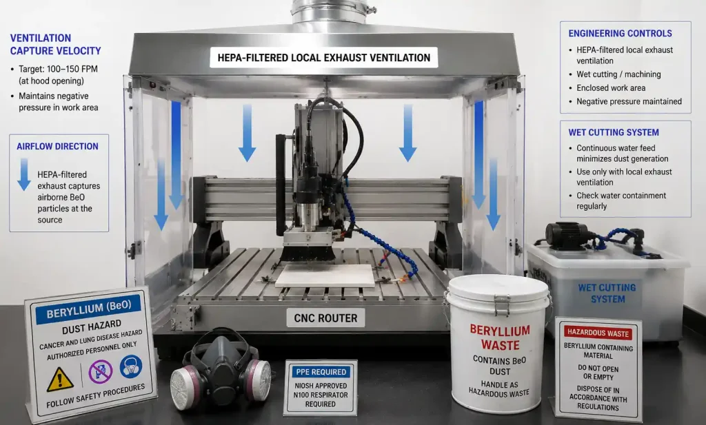
During any operation that may generate BeO dust or particles, operators must wear:
- NIOSH-approved N100 or P100 particulate respirators (not N95 masks, which provide insufficient protection)
- Disposable coveralls or dedicated work clothing that remains in the controlled area
- Nitrile or latex gloves for direct substrate contact
- Safety glasses with side shields to prevent eye exposure
Standard PCB assembly operations on intact BeO boards (component placement, soldering, inspection) require only nitrile gloves and safety glasses. Full respiratory protection is mandatory only when cutting, drilling, grinding, or sanding BeO material.
Work Area Controls
Designated BeO work areas must implement engineering controls before administrative controls:
- HEPA-filtered local exhaust ventilation at all machining stations, maintaining minimum 100 feet per minute capture velocity
- Wet cutting methods whenever feasible to suppress dust generation
- Separate storage areas with clear hazard labeling
- Prohibited eating, drinking, or smoking in BeO handling zones
- Daily HEPA vacuum cleaning of work surfaces (never use compressed air)
Beryllium-contaminated waste requires special disposal procedures. Scrap BeO material, used PPE, and HEPA vacuum contents must be collected in sealed, labeled containers and disposed through licensed hazardous waste contractors following EPA regulations.
Employee Medical Surveillance
OSHA beryllium standard mandates baseline and periodic medical examinations for workers with potential exposure above the action level. This includes pulmonary function tests and beryllium lymphocyte proliferation tests (BeLPT) to detect sensitization before progression to chronic disease.
3. Design Guidelines for BeO Substrate Applications
When specifying BeO substrates, design engineers must balance thermal performance requirements against safety compliance costs and supply chain constraints. BeO substrates are typically available in 0.25mm, 0.38mm, 0.5mm, and 0.635mm standard thicknesses.
Thermal Design Parameters
The following table compares key thermal properties relevant to high-power PCB design:
| Parameter | BeO Ceramic | Alumina (96%) | AlN Ceramic | Copper Core |
|---|---|---|---|---|
| Thermal conductivity (W/mK) | 250-300 | 24-28 | 170-200 | 390 |
| Coefficient of thermal expansion (ppm/°C) | 7.5 | 6.8 | 4.5 | 17 |
| Dielectric constant (1 MHz) | 6.7 | 9.8 | 8.8 | N/A |
| Dielectric strength (kV/mm) | 10-14 | 12-16 | 12-15 | Requires insulation |
| Max operating temperature (°C) | 500 | 400 | 350 | 180 |
| Relative cost | Very High | Low | High | Medium |
This comparison reveals BeO’s thermal advantage over alumina while showing that aluminum nitride (AlN) provides 70-80% of BeO’s conductivity without beryllium hazards. Cost analysis must include safety program expenses, not just material unit price.
For power dissipation above 50W in compact form factors, BeO enables junction-to-case thermal resistance reductions of 40-60% compared to alumina. However, designers should first evaluate whether AlN substrates or copper-core metal PCBs with appropriate insulation layers can meet thermal budgets without beryllium safety requirements.
Electrical Design Considerations
BeO’s dielectric constant of 6.7 is favorable for RF applications requiring controlled impedance. The material exhibits low loss tangent (0.0003 at 10 GHz), making it suitable for microwave circuits up to 40 GHz. Trace impedance calculations for BeO follow standard microstrip formulas with substrate height and dielectric constant inputs.
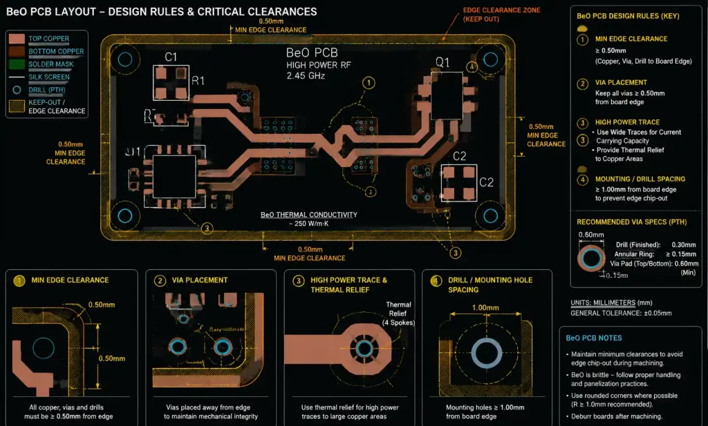
When routing high-power traces on BeO, maintain minimum 0.5mm clearance from board edges to prevent chip-out during handling. Via drilling in BeO requires carbide or diamond-coated bits and strict dust control measures.
4. Manufacturing Process Safety Requirements
PCB manufacturers handling BeO substrates must maintain certified beryllium safety programs with documented procedures, exposure monitoring, and employee training records subject to OSHA inspection.
Pre-Manufacturing Qualification
Before accepting BeO substrate orders, fabricators must verify:
- HEPA-filtered ventilation systems installed at all machining equipment
- Baseline air sampling data demonstrating exposure levels below action limit during similar operations
- Written beryllium safety program including emergency response procedures
- Trained workforce with completed beryllium awareness training
- Established relationships with certified hazardous waste disposal contractors
These infrastructure requirements create significant barriers to entry for many PCB manufacturers. Lead times for BeO substrate processing are typically 2-3 weeks longer than standard materials due to safety protocol compliance.
Process-Specific Safety Controls
The following table outlines required safety measures for each BeO PCB manufacturing step:
| Manufacturing Step | Dust Generation Risk | Required Controls | PPE Level |
|---|---|---|---|
| Incoming inspection | Minimal | Gloves, safety glasses | Standard |
| CNC routing/drilling | High | HEPA exhaust, wet cutting, full enclosure | N100 respirator, coveralls |
| Via laser drilling | Moderate | Enclosed laser system with fume extraction | Gloves, safety glasses |
| Copper patterning (etching) | Minimal | Standard wet process controls | Standard chemical PPE |
| Solder mask application | Minimal | Standard screen printing controls | Gloves, safety glasses |
| Scoring/depaneling | High | HEPA exhaust, wet cutting preferred | N100 respirator, coveralls |
| Final inspection | Minimal | Gloves, safety glasses | Standard |
| Packaging/shipping | Minimal | Individual board sleeves recommended | Gloves only |
The majority of safety risk concentrates in mechanical processes. Chemical processes (cleaning, plating, etching) pose standard PCB manufacturing hazards without additional beryllium-specific concerns.
Quality Control and Testing
Electrical testing of BeO boards follows standard procedures with one critical addition: test fixture contact points must be cleaned with HEPA vacuum between board changes to prevent beryllium cross-contamination to non-BeO products.
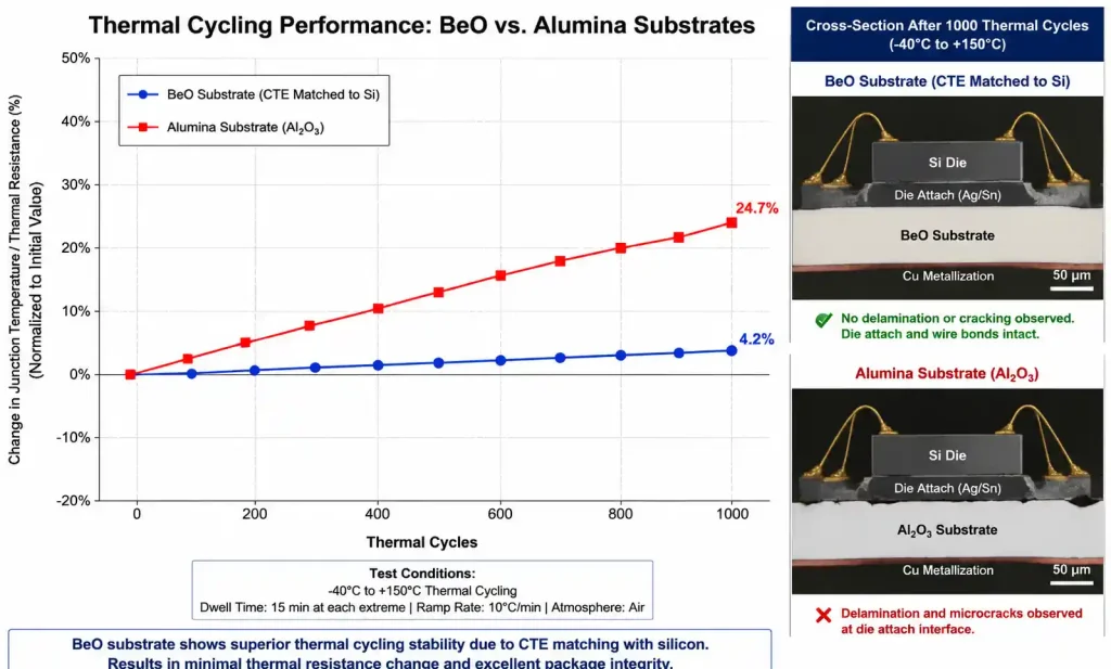
For applications requiring thermal cycling or temperature shock testing, BeO substrates demonstrate excellent reliability due to CTE match with silicon dies (7.5 vs 2.6 ppm/°C is closer than alumina’s 6.8 ppm/°C). Thermal test chambers processing BeO samples require dedicated HEPA filtration if substrate damage is possible.
5. Application Scenarios Where BeO PCBs Excel
Despite safety requirements increasing total cost of ownership, BeO substrates remain the material of choice for specific high-reliability applications where thermal performance is mission-critical.
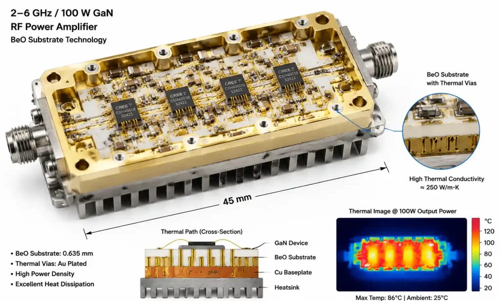
RF Power Amplifiers for Telecommunications
Base station power amplifiers operating at 50-100W continuous RF output require junction temperatures below 150°C to maintain linearity and prevent premature failure. BeO substrates enable compact PA designs meeting thermal requirements without forced air cooling in outdoor equipment enclosures.
Typical applications include:
- Cellular base station amplifiers (700 MHz to 3.5 GHz bands)
- Satellite communication uplink amplifiers
- Military radar transmitters requiring ruggedized construction
For these applications, BeO’s high thermal conductivity allows thermal resistance values of 0.5-0.8°C/W from device junction to heatsink, compared to 2-3°C/W achievable with standard alumina.
High-Power LED Arrays and Laser Diodes
Lighting applications requiring 10+ watts per LED emitter, or laser diode arrays for materials processing and medical equipment, benefit from BeO’s thermal management capability. Junction temperature directly affects LED efficacy and lifetime; every 10°C reduction extends L70 lifetime by approximately 2x.
Industrial LED applications on BeO include:
- UV curing systems (365-405nm high-power arrays)
- Horticultural lighting (high-density red/blue arrays)
- Automotive headlamp modules (laser-activated phosphor systems)
- Fiber laser pump diode arrays
Power Electronics and Hybrid Circuits
High-voltage DC-DC converters, motor drive inverters, and hybrid microwave integrated circuits (HMIC) use BeO when component density and thermal dissipation requirements exceed capabilities of alternative substrates.
Key design drivers for BeO selection include:
- Power density above 50 W/cm² in compact modules
- Operating ambient temperatures above 125°C
- High-voltage isolation requirements (>1000V) combined with thermal management
- Hermetic packaging compatibility for harsh environments
6. Alternative Materials Comparison
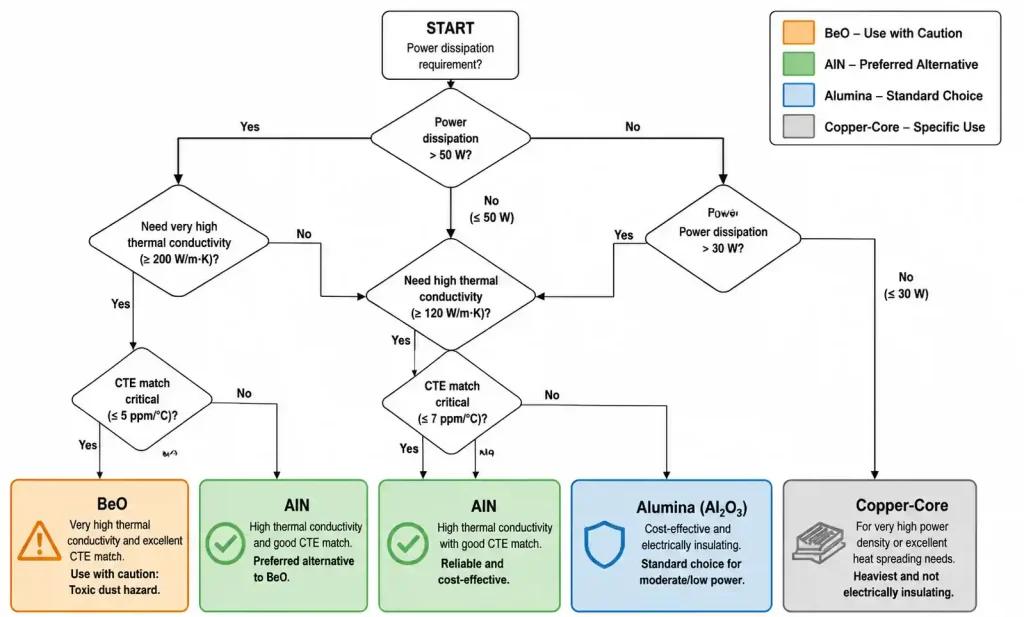
Before specifying BeO substrates, engineers should evaluate whether alternative thermal management materials can meet performance requirements without beryllium safety program costs.
Decision Framework by Application
Choose Aluminum Nitride (AlN) when:
- Thermal conductivity of 170-200 W/mK is sufficient (most applications below 30W)
- Project budget accommodates 3-5x material cost versus alumina
- CTE matching to silicon is critical (AlN = 4.5 ppm/°C)
- Supply chain prefers non-beryllium materials
Choose Copper-Core Metal PCB when:
- Application allows grounded metal core (cannot route signals through core)
- Operating temperatures remain below 150°C
- Dielectric isolation layer thermal resistance is acceptable
- High-frequency performance above 1 GHz is not required
Choose BeO only when:
- Thermal requirements exceed AlN capability and copper-core approach is unsuitable
- Application justifies safety program compliance costs
- Long-term supply chain for BeO is established
- End-of-life disposal procedures are defined
Cost Comparison Including Safety Compliance
Total cost of ownership for BeO substrates includes material, safety infrastructure, compliance monitoring, and disposal expenses:
| Cost Element | BeO Impact | Typical Cost Multiplier vs Alumina |
|---|---|---|
| Raw substrate material | High base cost | 15-25x |
| Manufacturing process time | Slower due to safety protocols | 1.5-2x labor |
| Safety equipment and PPE | Respirators, ventilation, monitoring | $20K-50K initial + $5K-10K annual |
| Employee training and medical surveillance | OSHA-mandated programs | $500-1000 per employee annually |
| Waste disposal | Hazardous waste classification | 10-20x standard scrap disposal |
| Total project cost (prototype) | Combined impact | 8-12x alumina baseline |
| Total project cost (production >1000 units) | Economies of scale improve ratio | 3-6x alumina baseline |
For prototype and low-volume production, BeO cost premium is severe. High-volume manufacturing (>5,000 units annually) reduces relative cost penalty as fixed safety infrastructure costs amortize across larger quantities.
7. FAQ
What makes beryllium oxide PCBs hazardous, and when is exposure a concern?
BeO substrates are hazardous only when mechanical processes (cutting, drilling, grinding) generate respirable beryllium-containing dust particles. Inhalation exposure can cause chronic beryllium disease, a serious lung condition. Intact BeO boards during normal handling, assembly, and operation pose minimal risk. The critical safety window is during substrate machining and end-of-life disposal when particle generation may occur.
Can standard PCB assembly equipment be used for BeO substrates?
Yes, standard SMT assembly equipment handles BeO substrates without modification. Reflow soldering, pick-and-place, and inspection processes proceed normally. BeO tolerates lead-free solder temperatures (260°C peak) without material degradation. Special safety measures are required only for mechanical operations like routing, drilling, or depaneling that create dust.
How does BeO thermal performance compare to aluminum nitride?
BeO provides thermal conductivity of 250-300 W/mK versus AlN’s 170-200 W/mK—approximately 40-50% higher. However, for most applications dissipating under 30-40W, AlN’s thermal performance is sufficient and avoids beryllium safety requirements. BeO shows clear advantage only in extreme power density applications or when minimizing thermal resistance is absolutely critical for reliability.
What disposal procedures are required for end-of-life BeO PCBs?
BeO substrates must be treated as hazardous waste containing beryllium. Disposal requires contracting licensed hazardous waste handlers familiar with beryllium-containing materials. Boards should be packaged to prevent breakage during transport. Never dispose of BeO substrates in standard electronic waste streams. Product documentation should clearly identify BeO content to ensure proper end-of-life handling.
Are there thickness or size limitations for BeO substrates?
Standard BeO substrate thicknesses are 0.25mm, 0.38mm, 0.5mm, and 0.635mm. Panel sizes are typically limited to 100mm x 100mm or 4″ x 4″ due to material brittleness and manufacturing handling constraints. Custom sizes are available but require longer lead times. Larger circuit areas may require tiling multiple BeO sections with proper thermal interface design.
What certifications do PCB manufacturers need to process BeO?
Fabricators must comply with OSHA 29 CFR 1910.1024 beryllium standard, which mandates written safety programs, exposure monitoring, engineering controls, employee training, and medical surveillance programs. Some manufacturers pursue voluntary certifications like ISO 45001 occupational health and safety management. Request documented evidence of beryllium safety program compliance before placing orders.
Can BeO substrates be reworked or repaired?
Rework of BeO assemblies is feasible but requires dust control measures. Component removal and replacement should use standard SMT rework techniques (hot air, focused IR). If substrate drilling or modification is needed during rework, full beryllium safety protocols (HEPA ventilation, N100 respirators) must be implemented. Document rework procedures in your manufacturing work instructions.
What RF performance advantages does BeO offer over alumina?
BeO’s lower dielectric constant (6.7 vs 9.8 for alumina) and very low loss tangent (0.0003 at 10 GHz) enable higher-frequency designs with lower insertion loss. The superior thermal conductivity also prevents hot spots that can shift RF characteristics in power amplifier circuits. For applications above 20 GHz or power levels exceeding 10W, BeO maintains stable electrical performance where alumina may experience thermal-induced drift.
8. Conclusion and Safety Compliance Recommendations
BeO PCBs deliver unmatched thermal management for high-power RF, laser diode, and power electronics applications where heat dissipation directly limits performance and reliability. The material’s 250-300 W/mK thermal conductivity enables compact designs that would overheat on alternative substrates.
However, specifying BeO commits your project to comprehensive safety compliance throughout manufacturing, assembly, and disposal phases. Before finalizing BeO in your design, verify that manufacturing partners maintain certified beryllium safety programs with documented OSHA compliance. Budget for 3-6x cost premium versus alumina in production volumes, with even higher ratios for prototypes.For most thermal management applications, aluminum nitride substrates or copper-core metal PCBs should be evaluated first. Reserve BeO specification for scenarios where thermal requirements genuinely exceed these alternatives—typically power densities above 50 W/cm² or applications where junction temperature reduction directly enables mission-critical performance improvements.
If your application requires BeO substrate evaluation, request design review support from PCB manufacturers with established beryllium safety programs. Many fabricators can provide thermal modeling services to confirm whether BeO’s performance advantages justify the safety compliance investment for your specific design.
Need assistance with BeO PCB thermal design or want to explore safer alternative materials? Contact our applications engineering team for design review and material selection guidance tailored to your power dissipation requirements.