
PCB Flying Probe Testing vs. Fixture Testing: Small Batch Production Cost-Benefit Analysis
PCB testing is one of those things nobody thinks about until it’s too late. Pick the wrong method and you’re either burning money on fixtures for a design that’s still changing, or you’re waiting 10 minutes per board for flying probe when you need 500 units shipped by Friday. Working with a PCB manufacturer that offers both testing options gives you the flexibility to choose the right method for each stage of production. This guide breaks down the real trade-offs—not theory, but actual cost and schedule numbers you can use.
Why This Decision Matters
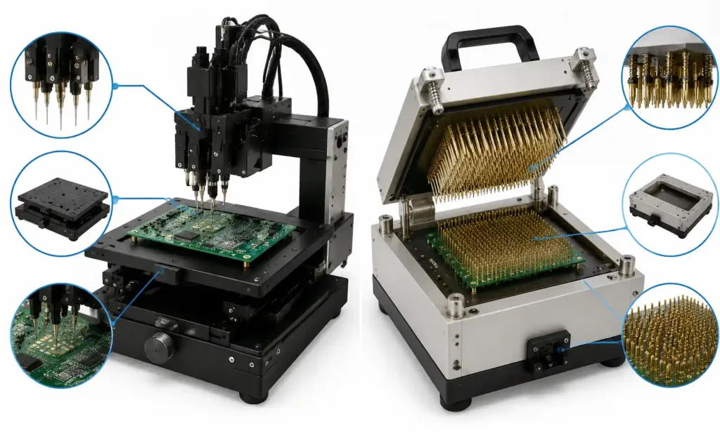
In high-volume production, fixture testing wins every time because the NRE amortizes over hundreds of thousands of boards. But for small batches—prototypes, NPI, or runs under 5,000 units—that math flips. A $3,000 fixture can easily exceed your entire testing budget.
Beyond cost, test method affects your ability to iterate quickly. If your design is still evolving, rebuilding fixtures each revision adds weeks of delay. Flying probe systems just reprograms from Gerber files. No hardware changes. No waiting.
| Factor | Flying Probe Testing | Fixture Testing |
|---|---|---|
| Setup cost | $0 fixture cost | $800–$8,000+ per fixture |
| Test programming | 2–8 hours from Gerber | 1–3 weeks for fixture design + fab |
| Batch size sweet spot | 1–5,000 units | 5,000+ units |
| Test coverage | 85–95% typical | 95–100% with proper DFT |
| Cycle time per board | 3–10 minutes | 15–60 seconds |
| Design iteration cost | $0 (reprogram only) | $500–$3,000+ fixture rework |
Flying probe uses moving test heads on X-Y stages to contact PCB nodes one at a time. Fixture testers use a fixed bed of spring-loaded pins that hit all test points simultaneously. That fundamental difference drives everything else.
Cost Structure Analysis
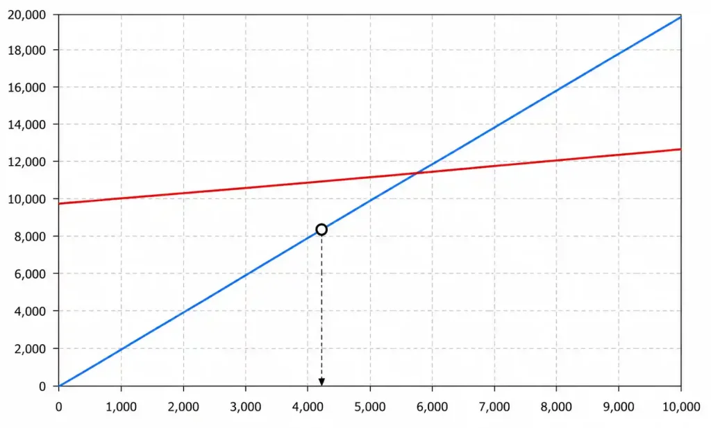
The breakeven point depends on three variables: fixture NRE cost, per-board test time, and production volume. For a typical 6-layer board with 200 test points, fixture costs run $2,000–$5,000. Flying probe takes 4–6 minutes per board; fixture does it in 30–45 seconds.
1,000-unit batch example:
Flying probe total: 1,000 × 5 min × $60/hr = $5,000 (no NRE)
Fixture total: $3,500 fixture + (1,000 × 40 sec × $60/hr) = $3,500 + $667 = $4,167
Fixture saves about $833 on that batch. But one engineering change during production adds $1,200–$2,500 in fixture rework—and suddenly flying probe wins again. For runs under 500 units, flying probe almost always wins on pure cost.
Test Coverage and Detection Capability
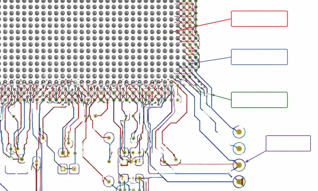
Flying probe achieves 85–95% coverage on designs without dedicated test points because probes can hit vias, component leads, and SMT pads directly. The limitation is physical access—you can’t probe under BGAs, shielded areas, or tight component clusters.
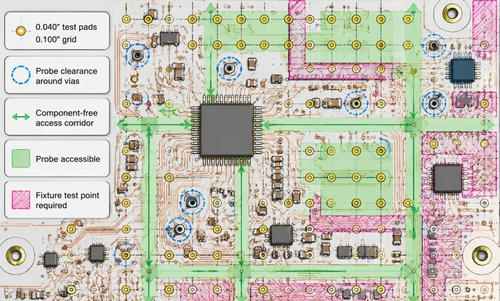
Fixture testing reaches 95–100% coverage when you design in proper test points per IPC-9252. Each test point needs a 0.040″–0.050″ pad with 0.100″ clearance from adjacent components. On high-density boards, that eats up real estate fast. Fixture pin pitch typically runs 0.050″–0.100″, making it tough for ultra-fine-pitch designs. For designs with very dense routing, HDI PCBs with mSAP process can achieve the fine geometries needed for advanced packages, but test access still requires careful DFT planning.
For boundary scan (JTAG), both methods work, but flying probe offers more flexibility for non-standard header placements.
Design Iteration Impact
Flying probe is made for agile development. When the schematic changes, test programs update from new Gerber files in 2–6 hours with zero tooling cost. Just reimport the netlist, verify probe access, and regenerate the sequence.
Fixture testing locks you in. Any component move, net name change, or test point shift requires fixture modification. Minor changes cost $500–$1,500 and take 3–7 days. Major redesigns may need a completely new fixture at full NRE.
| Design Change | Flying Probe Impact | Fixture Testing Impact |
|---|---|---|
| Component value change (same footprint) | 30 min reprogram | No change |
| Test point relocation | 1–2 hours | $800–$2,000 + 5–7 days |
| Board outline change | 2–4 hours | $2,000–$5,000 new fixture + 2–3 weeks |
| Add/remove nets | 1–3 hours | $1,200–$3,500 + 1–2 weeks |
For prototypes and NPI phases, flying probe removes the financial penalty for design exploration. When your design involves HDI flex PCB structures with 3+N+3 buildup, the ability to test without committing to fixtures is particularly valuable given the higher layer counts and tighter registration tolerances involved.
Throughput and Scheduling
Fixture testing’s speed advantage becomes obvious in volume. Fixture does 30–60 seconds per board; flying probe takes 3–10 minutes. For a 2,000-board run, that’s 10–15 hours (fixture) versus 100–333 hours (flying probe).
But cycle time alone misses the setup picture. Flying probe needs 2–8 hours for initial program development. Fixture testing needs 2–4 weeks for design, fabrication, and debug. If your production window is 3–5 days from Gerber release, only flying probe fits.
Most contract assemblers keep multiple flying probe testers with instant capacity. Fixture availability depends on the fixture shop’s queue—during peak seasons, lead times can stretch to 4–6 weeks.
When to Choose Which Method
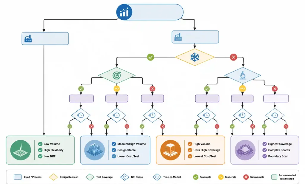
Choose flying probe when:
- Production volume is under 5,000 units per year
- Design is still evolving or in NPI phase
- Time-to-market is critical (testing within 1 week of design freeze)
- Board uses HDI stackups, blind/buried vias, or component-on-component
- Multiple PCB variants need testing (variant programming is trivial)
- 85–95% coverage meets your quality requirements
Choose fixture when:
- Production volume exceeds 5,000 units with stable design
- Design is locked with no expected ECOs
- Cycle time is critical for production throughput
- 100% test coverage is mandatory (automotive, medical, aerospace)
- Board already has IPC-9252 test points
- Fixture NRE amortizes to under $0.50 per board
Design for Testability by Method
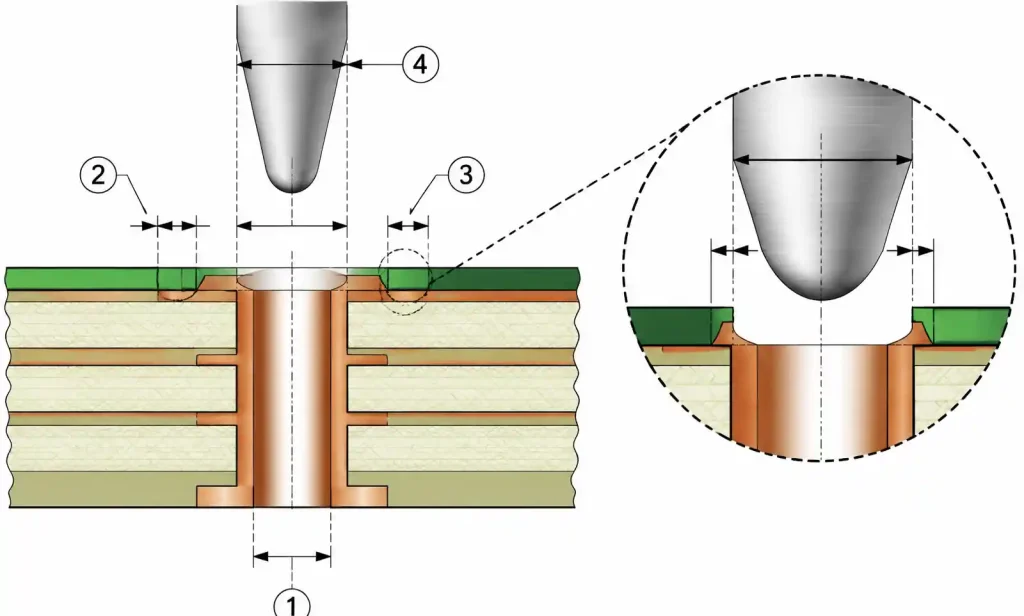
Flying probe DFT focuses on probe access rather than dedicated test points. Keep 0.020″–0.030″ clearance around vias and SMT pads used as probe targets. Avoid solder mask on test-critical nodes. Keep top and bottom surfaces accessible—no conformal coating until after test. Via sizes should be ≥0.012″ finished hole for reliable probe contact.
For designs that might scale from flying probe to fixture later, implement a test point strategy that works for both: place 0.040″ test pads on 0.100″ grid where space allows, route critical nets to probe-accessible locations, and document probe access limitations in assembly drawings.
Hybrid Strategies
Some manufacturers stage their approach: flying probe for prototypes and pilot runs (1–500 units), then amortize fixture cost once production hits 1,000+ units and the design is frozen. This captures flying probe’s flexibility during NPI while gaining fixture efficiency in volume.
Another hybrid: flying probe for comprehensive electrical testing, combined with a lower-cost fixture for functional testing. The fixture only contacts power, ground, and key I/O signals—reducing complexity and cost by 60–70% compared to full in-circuit test fixtures.
FAQ
Can flying probe test BGAs and QFNs without test points?
Flying probe can test BGA and QFN perimeter nets that route to vias or other accessible nodes within 1–2 component body lengths. Internal BGA balls with no external routing cannot be probed without dedicated test vias. For packages >0.5mm pitch, via-in-pad fanouts provide access. For fine-pitch BGAs (<0.5mm), boundary scan (JTAG) is the preferred solution regardless of test method.
How long does fixture fabrication take?
Standard lead time is 2–3 weeks from approved CAD data. Rush fixtures (1 week) cost 30–50% more. Complex fixtures with vacuum hold-down, high pin counts (>1,000 points), or custom tooling may take 4–5 weeks. Get fixture quotes early in your NPI timeline.
Does flying probe work with conformal coating?
No. Flying probe must happen before conformal coating—probes can’t penetrate coating materials. Process sequence: PCB assembly → flying probe test → rework (if needed) → conformal coating → final functional test.
Which test method meets IPC Class 3 medical and aerospace requirements?
IPC Class 3 doesn’t mandate a specific test method, but it requires 100% electrical verification of all nets and components. Both flying probe and fixture can meet Class 3 if coverage reaches 100%. Plan DFT early to ensure either method achieves full coverage—this typically means adding test points even with flying probe.
Conclusion
For small batch production under 5,000 units, flying probe testing usually delivers better cost-effectiveness and schedule performance. Zero NRE, rapid test program development, and design flexibility make it the default choice for prototypes, NPI builds, and low-to-medium volume production.
Fixture testing becomes financially attractive when production exceeds 5,000 units annually and your design is stable enough to justify the upfront tooling investment. The throughput advantage and maximum test coverage make fixtures the right choice for mature products in volume manufacturing.
Before committing, calculate your specific breakeven point using actual batch sizes and fixture quotes. If you’re early in product development with uncertain volume, start with flying probe and preserve the option to transition to fixtures once production scales and design stabilizes. Partnering with a PCB manufacturer that supports both test methods gives you the flexibility to adapt your testing strategy as your product matures.