
What is HDI PCB? Everything You Need to Know in 2026
High-density interconnect (HDI) PCBs now dominate over 70% of smartphone mainboard designs and are rapidly expanding into wearables, medical implants, and automotive ADAS systems. Understanding HDI technology is no longer optional for hardware engineers and product designers. This guide covers HDI PCB fundamentals, via types, layer stackup strategies, and manufacturing capabilities.
What Is HDI PCB?
HDI PCB is a high-density interconnect printed circuit board featuring microvias smaller than 0.15mm in diameter, fine-pitch traces as narrow as 3mil (75μm), and sequential build-up layer construction. This technology enables significantly higher component density and improved electrical performance compared to traditional through-hole boards.
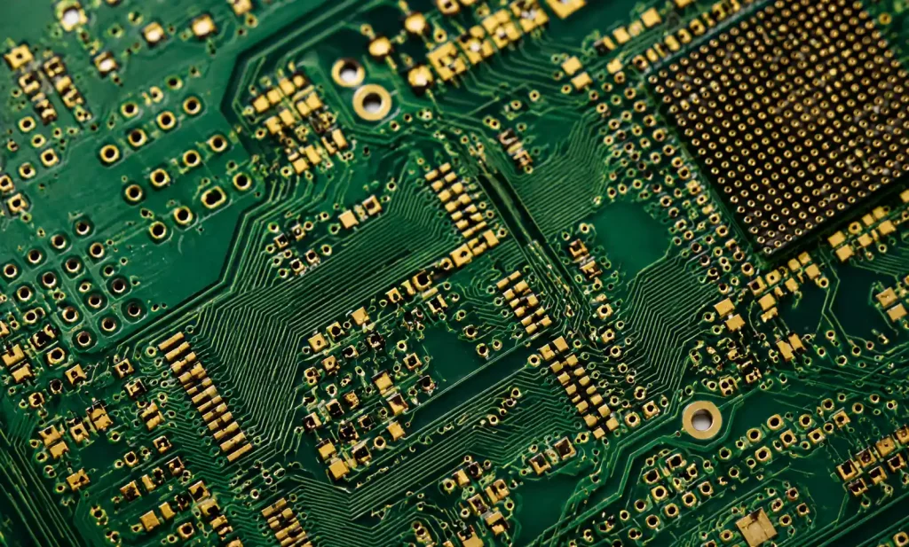
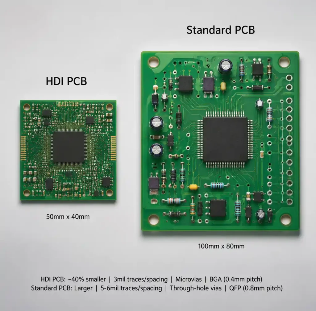
The defining characteristic is the microvia—a laser-drilled hole connecting adjacent layers without penetrating the entire board. These microvias allow routing between dense BGA pads with 0.4mm pitch or finer—impossible with standard mechanical drilling limited to 0.3mm. HDI delivers 30-40% board size reduction while improving signal integrity for frequencies above 1 GHz through shorter signal paths and reduced EMI.
HDI PCB Via Types and Structures
Via architecture determines routing density, layer count, manufacturing cost, and signal integrity performance.
Blind Vias
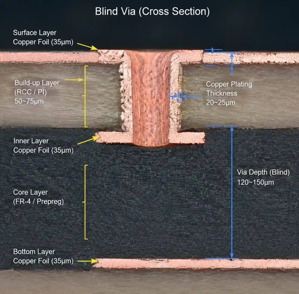
Blind vias connect an outer layer to inner layers without penetrating the entire board. They enable via-in-pad design where the via sits directly beneath component pads, eliminating spacing constraints. Blind vias add 15-25% to manufacturing cost but provide substantial routing efficiency benefits.
Buried Vias
Buried vias connect only internal layers and remain hidden within the stackup. They don’t consume surface area, preserving space for component placement. Manufacturing requires sequential lamination where inner layer pairs are drilled, plated, and laminated before adding outer layers.
Microvias
Microvias are laser-drilled blind vias with diameters from 0.075mm to 0.15mm. They can be stacked (aligned vertically) or staggered (offset between layers). Stacked vias provide direct connections but require advanced processes; staggered vias distribute stress better for thermal cycling applications.
HDI Build-Up Structures Explained
HDI PCBs are classified by build-up structure, which describes how many sequential lamination layers exist on each side of the core.
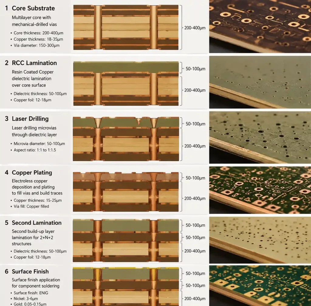
1+N+1 Structure: One build-up layer on each side of a multilayer core. Most common and cost-effective HDI configuration. A 4-layer core with one build-up each side creates an 8-layer HDI. Costs 40-60% more than standard PCBs.
2+N+2 Structure: Two build-up layers each side, enabling higher density and more complex routing. Common in flagship smartphones and advanced wearables. Costs 70-100% more than standard PCBs.
Any-Layer HDI: Microvias can connect any layer to any other layer. Maximum routing density for ultra-high-end applications. Costs 2-3× higher than standard PCBs but enables otherwise impossible designs.
| Build-Up Type | Structure | Typical Layers | Cost vs Standard | Applications |
|---|---|---|---|---|
| 1+N+1 | 1 build-up each side | 6-10 layers | +40-60% | Smartphones, tablets, consumer electronics |
| 2+N+2 | 2 build-up each side | 8-14 layers | +70-100% | Flagship phones, wearables, medical devices |
| 3+N+3 | 3 build-up each side | 12-18 layers | +100-150% | High-end servers, telecom infrastructure |
| Any-Layer | Unrestricted via placement | 10-20+ layers | +150-200% | Advanced medical, aerospace, military |
HDI PCB vs Standard PCB
| Parameter | HDI PCB | Standard PCB |
|---|---|---|
| Minimum Via Size | 0.075-0.15mm (laser) | 0.3mm (mechanical) |
| Minimum Trace/Space | 3/3 mil (75/75μm) | 5/5 mil (125/125μm) |
| Via Types | Blind, buried, microvia | Through-hole only |
| Component Pitch | 0.4mm BGA capable | 0.8mm+ BGA typical |
| Board Thickness | 0.4-1.6mm typical | 1.0-2.4mm typical |
| Layer Count | 6-50+ layers | 2-16 layers |
| Signal Integrity | Excellent (short paths) | Good (longer paths) |
| Size Reduction | 30-40% smaller | Standard size |
| Cost | Higher | Lower |
| Lead Time | 10-18 days | 7-12 days |
Choose HDI when your design requires component pitch below 0.5mm, board thickness under 1.2mm, impedance-controlled routing above 500 MHz, or when size reduction drives product differentiation.
Key Design Considerations
Via Design Rules
Microvia diameter typically ranges from 0.1mm to 0.15mm with annular ring of at least 0.05mm. Pad diameter should be 0.2mm to 0.25mm for a 0.1mm microvia. Stacked microvias require copper filling. Blind via depth should not exceed diameter by more than 1:1 aspect ratio.
Layer Stackup Strategy
HDI stackups require careful impedance planning because thin dielectric layers create different impedance profiles. Work with your PCB manufacturing partner to validate stackup calculations. Place power and ground planes adjacent to signal layers. Typical build-up dielectric thickness is 50-100μm versus 200-400μm in cores.
Design for Manufacturing
Via-in-pad requires via plugging or copper filling. Specify clearly in fabrication notes. Minimum trace width is 75μm (3mil) with 75μm spacing. Maintain 0.15mm clearance from microvia pads to adjacent traces. Use teardrops on microvia connections.
Manufacturing Process
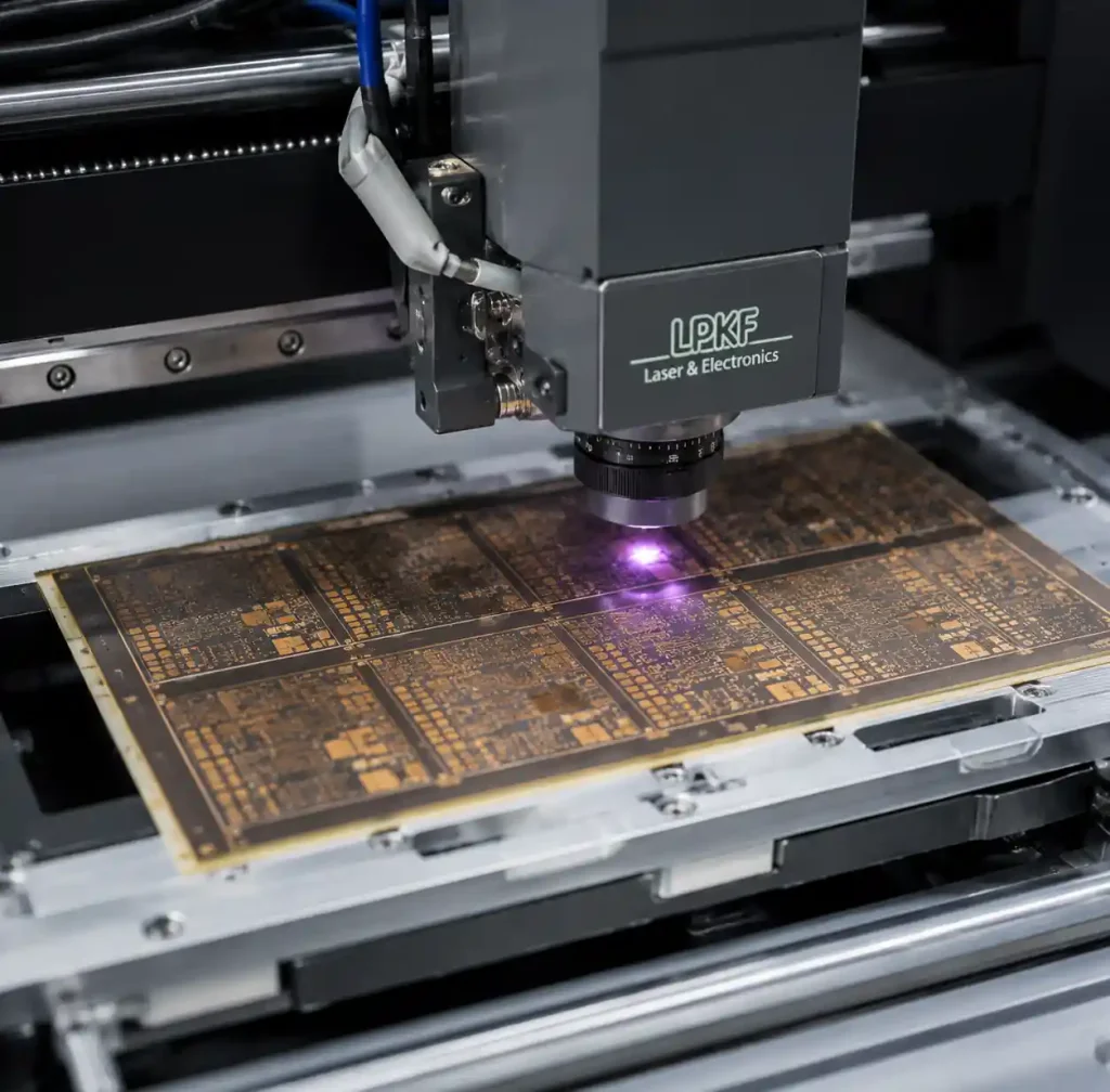
HDI manufacturing begins with a conventional multilayer core. After core fabrication, manufacturers apply a thin dielectric layer using resin-coated copper (RCC). Laser drilling creates microvias with ±15μm positioning accuracy. Electroless copper deposition coats via walls, followed by pattern plating. For 2+N+2 structures, the process repeats.
Final processing includes solder mask, surface finish (typically ENIG), silkscreen, and electrical testing. HDI boards require flying probe testing and automated optical inspection (AOI) of all microvia locations. Lead time: 10-18 days depending on complexity. Andwin Circuits offers fast turnaround HDI PCB manufacturing up to 50 layers.
Applications Across Industries
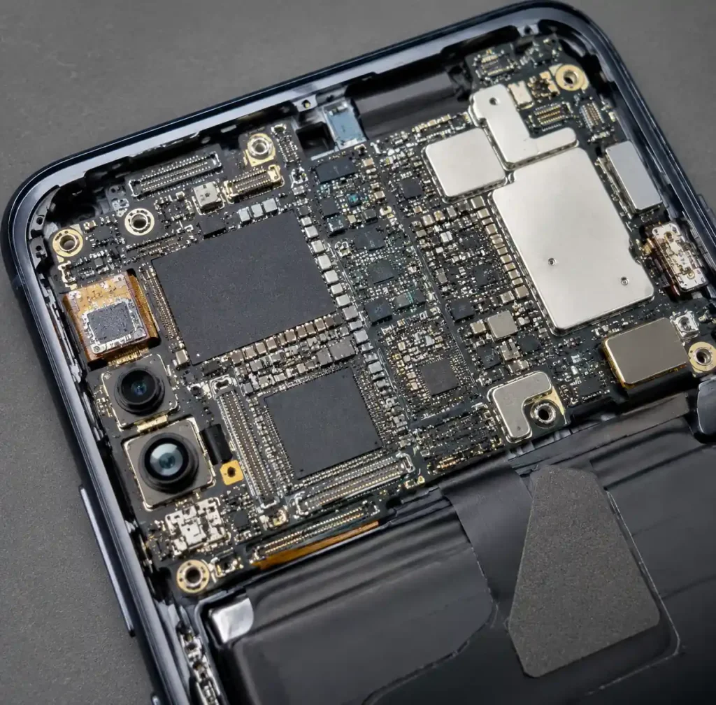
Consumer Electronics: Smartphones use 2+N+2 or 3+N+3 structures. Tablets, smartwatches, and wireless earbuds depend on HDI for wearable sizes.
Medical Devices: Implantable devices (pacemakers, neurostimulators) use HDI meeting IPC-6012 Class 3. Portable diagnostic equipment leverages HDI for handheld form factors.
Automotive Electronics: ADAS radar, camera systems, and sensor fusion use HDI with IATF 16949 quality. EV power electronics adopt HDI with heavy copper (3-6oz) in power layers combined with fine-line signal layers.
Telecommunications: 5G infrastructure requires HDI for high-frequency signals up to 40 GHz with precise impedance control.
Cost Factors
Layer Count and Build-Up: 1+N+1 costs 40-60% more than standard. Each additional build-up layer adds 25-35%.
Microvia Count and Type: Thousands of microvias increase cost. Stacked microvias with copper filling add 15-25% premium.
Material Selection: High-frequency low-loss substrates add 30-50%. High-Tg materials add 10-15%.
Surface Finish: ENIG is standard for HDI, costing 20-30% more than HASL but providing flat surfaces for fine-pitch assembly.
Reduce costs by minimizing build-up layers, using standard FR-4 when possible, and optimizing for your manufacturer’s process capabilities.
FAQs
What does HDI stand for in PCB?
HDI stands for High-Density Interconnect, referring to boards with higher wiring density per unit area using microvias, fine traces, and advanced build-up structures.
What is the minimum via size for HDI PCB?
Minimum microvia size is typically 0.075mm to 0.1mm diameter. Pad diameter is 0.2mm to 0.25mm with 0.05mm annular ring. Advanced manufacturers can achieve 0.05mm microvias.
How many layers can HDI PCB have?
HDI PCBs range from 6 to 50+ layers. Consumer electronics typically use 8-14 layers. Andwin Circuits manufactures HDI PCBs up to 50 layers.
What is the difference between HDI and standard PCB?
HDI uses laser-drilled microvias (0.075-0.15mm) enabling blind/buried vias, while standard PCBs use mechanical-drilled through-hole vias (0.3mm minimum). HDI supports finer traces (3mil vs 5mil) and better signal integrity.
What are the types of HDI vias?
HDI vias include blind vias (outer to inner), buried vias (inner only), and microvias (laser-drilled under 0.15mm). Microvias can be stacked or staggered.
Conclusion
HDI PCB technology delivers 30-40% size reduction and superior signal integrity for modern electronic devices. Understanding via structures, build-up configurations, and design rules helps you specify the optimal technology for your product. Whether you need 1+N+1 for moderate density or any-layer HDI for extreme miniaturization, selecting the right configuration balances performance, cost, and manufacturability.
If you need high-quality HDI PCB manufacturing, Andwin Circuits offers advanced capabilities up to 50 layers with fast delivery in 10 days, certified to ISO 9001, IATF 16949, and IPC standards. Contact us today for custom HDI PCB solutions and competitive factory-direct pricing.