
Telecom PCB Design for 5G Infrastructure: High-Frequency Considerations
If you want to design reliable PCBs for 5G base stations and telecommunications infrastructure, then you will need to understand high-frequency materials, impedance control techniques, loss tangent requirements, and thermal management strategies that ensure signal integrity at mmWave frequencies.
5G infrastructure operates at significantly higher frequencies than previous generations, with FR2 bands extending from 24 GHz to 52 GHz for mmWave applications. Signal attenuation increases dramatically with frequency, making material selection and design optimization critical. According to industry analysis, improper PCB design accounts for 35% of 5G base station field failures, with signal integrity and thermal issues being the primary causes.
This guide covers essential high-frequency considerations for telecommunication PCB design, including material selection, stackup optimization, via structures, and thermal management for deployed 5G infrastructure.
High-Frequency PCB Materials for 5G
Material selection directly determines signal integrity and insertion loss in 5G infrastructure PCBs. Standard FR4 (Dk 4.2-4.5, Df 0.02) exhibits excessive signal loss above 10 GHz, making it unsuitable for mmWave applications.
Rogers High-Frequency Laminates
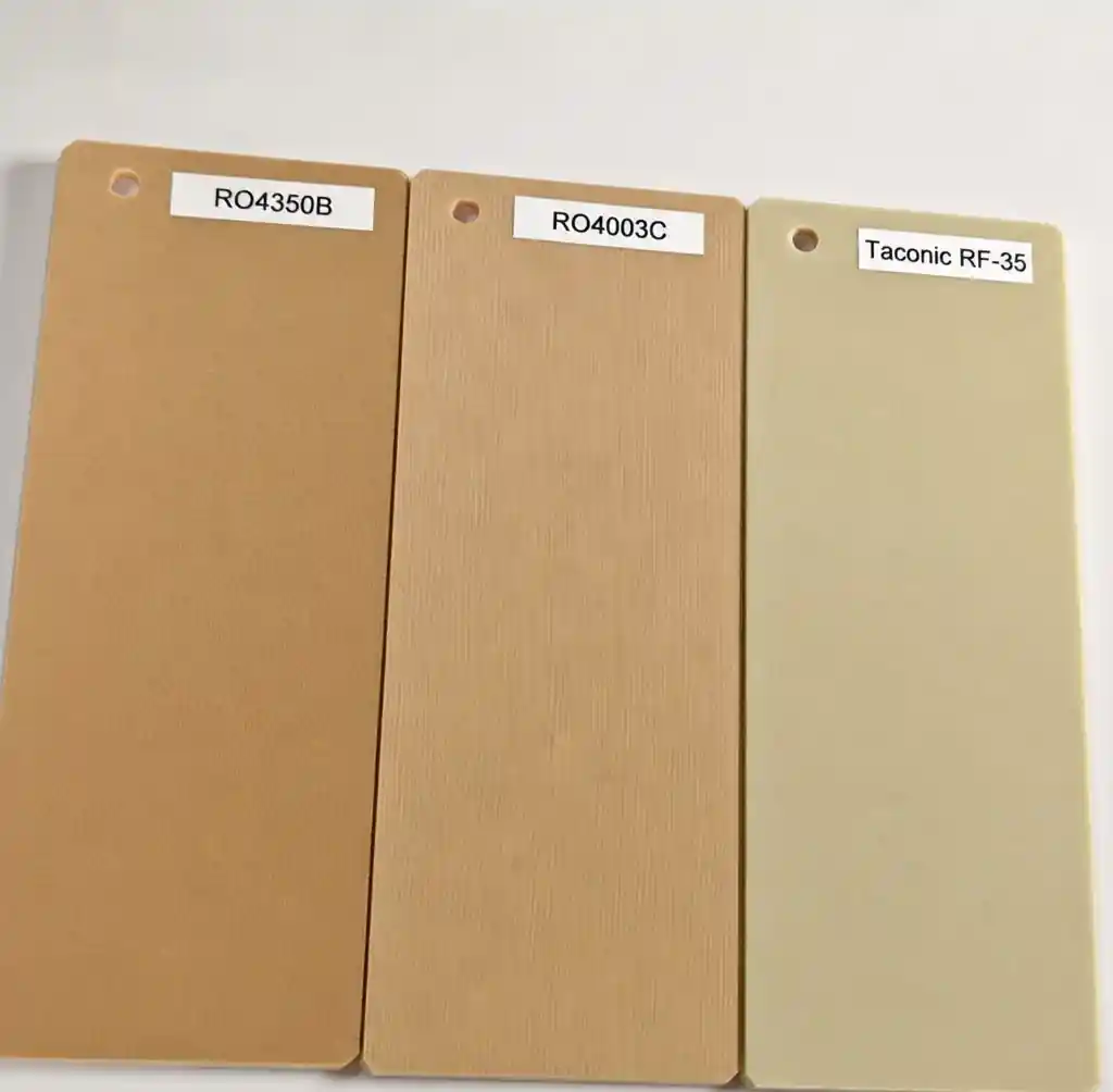
Rogers materials dominate 5G designs due to stable dielectric properties and low loss. RO4350B (Dk 3.48, Df 0.0037 at 10 GHz) provides excellent performance for sub-6 GHz bands. RO4003C (Dk 3.38, Df 0.0027) delivers lower loss for mmWave above 24 GHz. RO3003 (Dk 3.00, Df 0.0013) serves demanding 28 GHz and 39 GHz applications. This PTFE-based material maintains stable properties from -40°C to +125°C for outdoor equipment.
Taconic RF Laminates
Taconic RF-35 (Dk 3.50, Df 0.0025) offers cost-effective alternative for moderate-frequency applications. TLY-5 (Dk 2.20, Df 0.0009) serves ultra-high-frequency designs above 40 GHz. Specify Taconic materials when budget constraints prevent premium Rogers laminates.
The table below compares key properties of common high-frequency materials for 5G telecom applications:
| Material | Dk at 10 GHz | Df at 10 GHz | Thermal Conductivity (W/m·K) | CTE (ppm/°C) | Typical Application |
|---|---|---|---|---|---|
| FR4 (Standard) | 4.2-4.5 | 0.020 | 0.3 | 14-17 | Not recommended for 5G |
| Rogers RO4350B | 3.48 | 0.0037 | 0.69 | 10-14 | Sub-6 GHz, FR1 bands |
| Rogers RO4003C | 3.38 | 0.0027 | 0.64 | 11-14 | mmWave FR2 bands |
| Rogers RO3003 | 3.00 | 0.0013 | 0.50 | 17-24 | Ultra-high frequency |
| Taconic RF-35 | 3.50 | 0.0025 | 0.52 | 17-24 | Cost-effective FR1/FR2 |
| Taconic TLY-5 | 2.20 | 0.0009 | 0.38 | 20-28 | Above 40 GHz |
Loss Tangent and Dielectric Properties
Loss tangent (Df) quantifies RF energy conversion to heat during signal propagation. At 28 GHz, a 50mm microstrip on FR4 (Df 0.02) exhibits 1.3 dB insertion loss, while RO4003C (Df 0.0027) shows only 0.17 dB loss.
Dielectric constant (Dk) stability affects impedance control and signal timing. Specify materials with Dk tolerance ±0.05 for controlled impedance designs. Rogers RO4350B maintains TCDk of -40 ppm/°C, ensuring consistent performance across -40°C to +85°C.
Choose RO4350B below 6 GHz, RO4003C for 6-28 GHz, and RO3003 above 28 GHz. Rogers materials cost 3-5× standard FR4, while ultra-low-loss PTFE reaches 8-10× FR4 pricing.
Impedance Control for 5G Signals
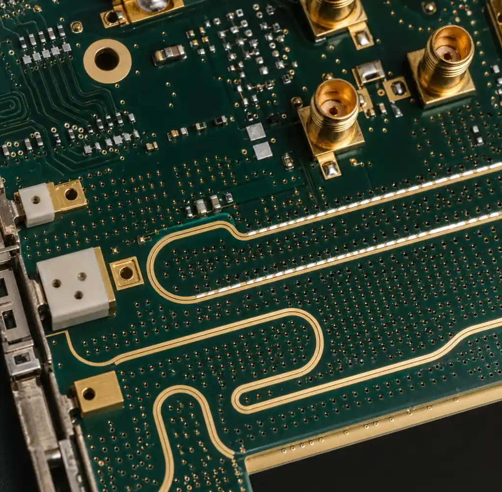
5G RF circuits require precise 50Ω impedance matching to minimize reflections and maximize power transfer. Microstrip places signal traces on outer layers with ground plane below, while stripline embeds signals between two ground planes for better isolation.
Calculate microstrip impedance using: Z0 = (87/√(Dk+1.41)) × ln(5.98h/(0.8w+t)). For 50Ω on RO4350B (Dk 3.48) with 0.2mm dielectric and 1oz copper, trace width is approximately 0.4mm.
High-speed digital interfaces use differential pairs for noise immunity. Maintain consistent spacing (2-3× trace width) and route pairs together. For 100Ω differential on RO4350B, use 0.15mm trace width with 0.15mm spacing on 0.2mm dielectric.
Manufacturers guarantee ±10% impedance tolerance (±5Ω for 50Ω) on controlled impedance PCB designs. Specify testing per IPC-TM-650 using time-domain reflectometry (TDR). Tighter ±5% tolerance increases cost by 30-50%.
Layer Stackup Design for RF Performance
PCB stackup architecture impacts signal integrity, EMI performance, and thermal management. Hybrid stackups combine high-frequency materials for RF layers with FR4 for digital/power layers, optimizing cost while maintaining performance.
A typical 10-layer 5G design uses RO4003C for top two RF layers with FR4 for remaining eight layers. Use thin bonding layers (0.075-0.1mm) and verify CTE compatibility. Rogers RO4000 series (CTE 10-14 ppm/°C) closely matches FR4 (14-17 ppm/°C), minimizing thermal stress.
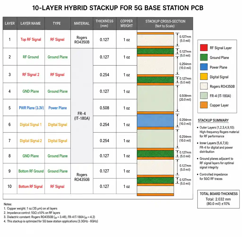
Place RF traces on outer layers with adjacent ground planes creating microstrip transmission lines. Multiple ground planes every 2-3 layers provide low-impedance return paths and effective shielding. Avoid splitting ground planes under high-frequency traces. Space power and ground planes closely (0.1-0.2mm) for low-inductance decoupling.
Via Optimization for mmWave Frequencies
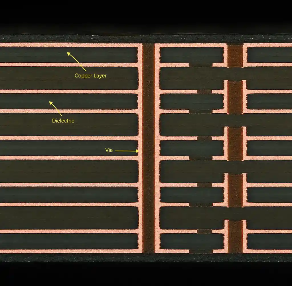
Vias introduce impedance discontinuities and parasitics that degrade signal integrity at mmWave frequencies. Through-hole vias create stubs that resonate at high frequencies. Use back-drilling to remove unused via barrels below the last connected layer, eliminating stub resonance.
Blind and buried vias eliminate stubs entirely but increase cost by 25-40%. Most designs use back-drilled through-holes as cost-effective compromise.
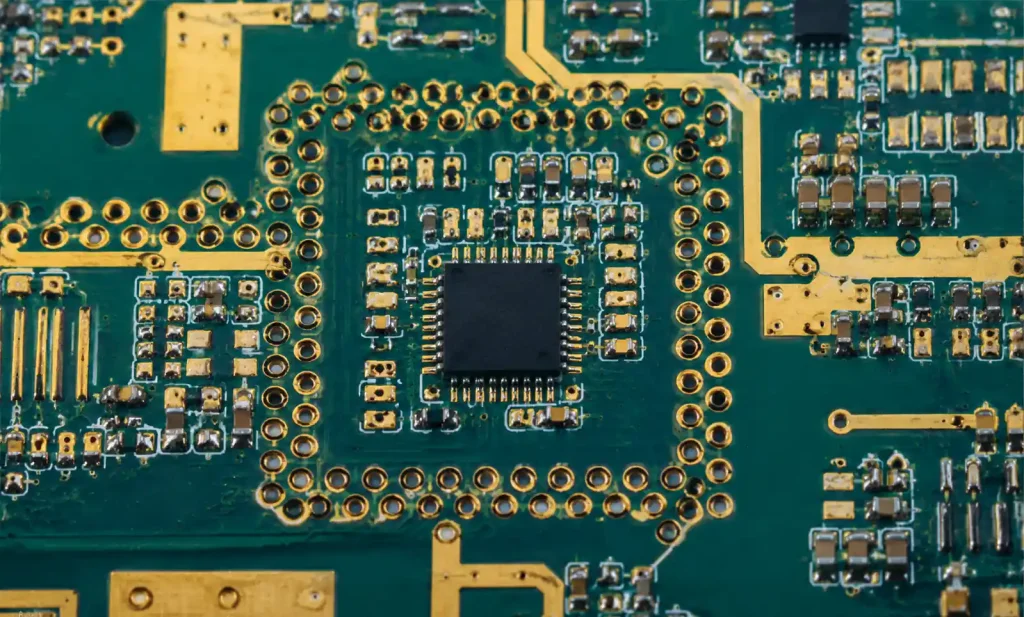
Ground vias surrounding signal vias create shields containing electromagnetic fields. Via fence spacing should be less than λ/20. At 28 GHz, via spacing should not exceed 0.28mm. Practical designs use 0.5-1.0mm spacing balancing shielding and routing density.
Connect ground vias to multiple layers minimizing impedance. Multiple parallel vias reduce inductance: L_total = L_single / N. Differential vias require symmetric placement with equal trace lengths and proper spacing maintaining differential impedance.
Thermal Management for High-Power 5G
5G base stations generate significant heat from power amplifiers operating at 40-60% efficiency. A typical massive MIMO base station with 64 transmit chains generates 500-1000W requiring aggressive thermal management.
Thermal Vias and Heavy Copper
Thermal vias transfer heat through PCB to heatsinks. Use 0.3-0.5mm diameter vias spaced 0.8-1.2mm under high-power components. Each via contributes 30-50°C/W thermal resistance. A 10W power amplifier requires 15-25 thermal vias maintaining junction temperature below 125°C.
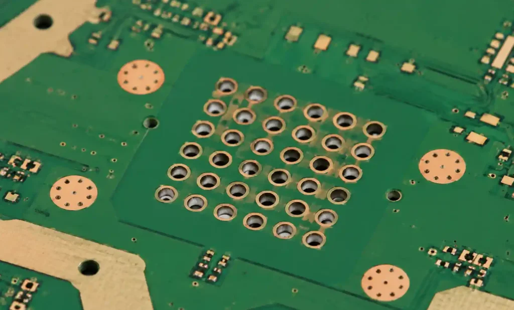
For highest power densities, metal core PCB provides thermal conductivity 50-200× higher than FR4. 5G power distribution requires heavy copper (3-6oz) minimizing resistive losses. A 50A supply using 1oz copper requires 8mm trace width, while 4oz copper achieves same performance with 2mm width.
The table below shows recommended copper weights and thermal strategies:
| Application | Current Range | Copper Weight | Thermal Strategy |
|---|---|---|---|
| Low power RF | <2A | 0.5-1oz | Minimal thermal vias |
| Power amplifiers | 2-10A | 2-3oz | Via arrays under devices |
| DC/DC converters | 10-30A | 3-4oz | Thermal vias + heatsinks |
| High-power PA | 30-50A+ | 4-6oz | MCPCB or thermal board |
Perform thermal simulation using Ansys Icepak or Mentor FloTHERM before finalizing designs. Simulation predicts junction temperatures and validates thermal management under worst-case conditions.
Design Guidelines for 5G Telecom PCBs
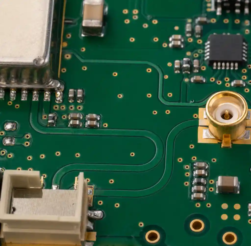
Route high-frequency traces as short as possible minimizing insertion loss. Each millimeter of microstrip on RO4003C adds 0.003 dB loss at 28 GHz. Keep critical RF paths under 50mm. Avoid 90-degree corners; use chamfered or curved bends with radius at least 3× trace width.
Maintain 3× trace width spacing between RF traces minimizing crosstalk. For critical signals, increase spacing to 5-10× width or place ground traces between signals.
Place RF components with shortest interconnections. Position power amplifiers near board edges or thermal vias for heat removal. Maintain 5mm clearance between high-power RF and sensitive low-noise amplifiers unless shielded.
Use continuous ground planes and minimize splits. Shield cans over RF circuits prevent radiation. Edge plating and via fences improve EMC performance for outdoor equipment meeting FCC or CE requirements.
Quality Standards and Testing
Specify IPC-6012 Class 3 for critical telecom applications requiring highest reliability. 100% electrical testing verifies continuity, isolation, and impedance. PCB E-test catches manufacturing defects before assembly.
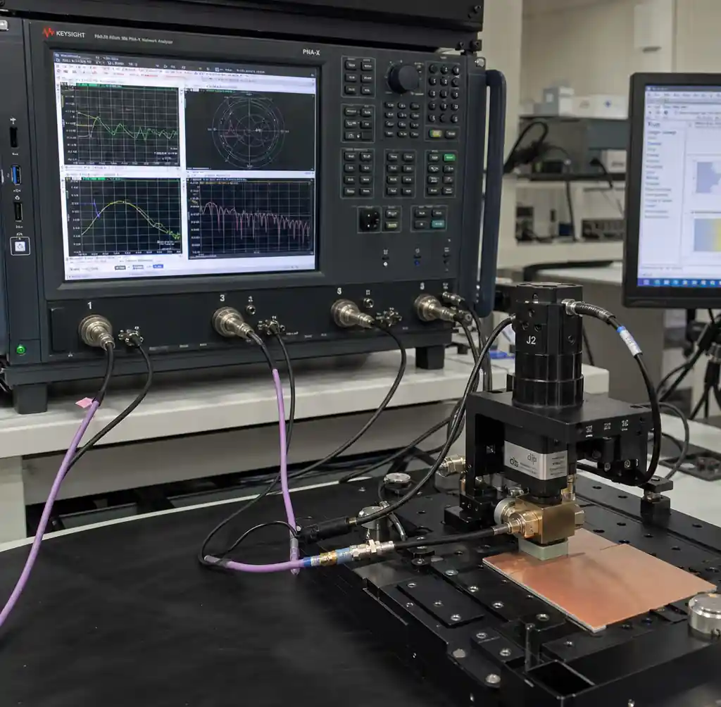
Impedance testing per IPC-TM-650 uses TDR to verify ±10% tolerance. S-parameter measurement characterizes insertion loss, return loss, and isolation. Temperature cycling (-40°C to +125°C) validates material selection and interface reliability.
FAQs
What materials are best for 5G mmWave PCBs above 24 GHz?
Rogers RO4003C (Dk 3.38, Df 0.0027) and RO3003 (Dk 3.00, Df 0.0013) provide excellent performance for mmWave frequencies. RO3003 offers lower loss above 28 GHz. Taconic TLY-5 provides cost-effective performance for budget-sensitive designs.
How thick should dielectric layers be for 50Ω impedance at 28 GHz?
Typical dielectric thickness ranges 0.1-0.3mm depending on material Dk. RO4003C with 0.2mm thickness requires approximately 0.38mm trace width for 50Ω microstrip, balancing manufacturing feasibility and loss performance.
Can FR4 be used for any 5G applications?
FR4 (Df 0.02) exhibits excessive loss above 6 GHz for RF signal paths. However, FR4 works well for digital processing, power distribution, and mechanical support in hybrid stackups where RF signals use high-frequency materials.
What copper weight should I specify for 5G power amplifiers?
Power amplifier stages require 2-4oz copper depending on current levels. Applications above 50W may need 4-6oz copper or metal core PCB for thermal management. Standard 1oz copper suffices for low-power RF under 2W.
How many thermal vias are needed under a 10W power amplifier?
Plan for 15-25 thermal vias (0.3-0.5mm diameter) under high-power components. Each via contributes 30-50°C/W thermal resistance. Thermal simulation determines optimal number based on power, temperature limits, and heatsink performance.
What impedance tolerance is required for 5G infrastructure?
Standard ±10% tolerance (±5Ω for 50Ω) meets most requirements when matching networks compensate for variations. Critical applications can specify ±5% tolerance at increased cost. Consistent impedance matters more than absolute value.
Conclusion
Designing reliable PCBs for 5G telecommunications infrastructure requires careful material selection, precise impedance control, optimized via structures, and aggressive thermal management. High-frequency materials like Rogers RO4003C and RO3003 provide the low loss tangent and stable dielectric properties essential for mmWave signal integrity, while hybrid stackups balance performance and cost. Proper thermal design using via arrays, heavy copper, and metal core construction ensures reliable operation of high-power amplifiers.
If you need high-quality telecommunication PCBs for 5G infrastructure, Andwin Circuits offers advanced manufacturing capabilities up to 50 layers with controlled impedance testing and fast turnaround in 7 days. Our facility is certified to ISO 9001 and IPC standards, with extensive experience in RF and high-frequency designs for telecommunications.
Contact us today for custom PCB solutions, technical specifications, and competitive factory-direct pricing for your 5G infrastructure project.