
Flexible Hybrid Electronics (FHE): Combining Flex PCB with Printed Electronics
Most wearable devices fail not because the sensor stopped working, but because the circuit couldn’t survive being worn. A rigid PCB cracks when fabric stretches. A fully printed circuit degrades when the wearer sweats. The electronics that bend with human motion need something neither traditional PCBs nor printed circuits deliver alone.
Flexible hybrid electronics (FHE) solves this by combining the performance of silicon ICs with the conformability of printed substrates. It places rigid chips where processing power matters and prints sensors where flexibility is required. This architecture is why medical patches can now monitor glucose continuously and why smart labels survive shipping without adding weight.
What is Flexible Hybrid Electronics?
FHE integrates conventional semiconductor components—microcontrollers, memory chips, power management ICs—onto flexible substrates using printed interconnects and sensors. The phrase “print what you can, place what you can’t” defines the approach: additive manufacturing creates passive elements, conductive traces, and sensing layers, while pick-and-place assembly handles active components that demand silicon-level performance.
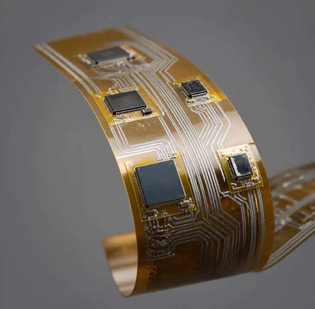
The key distinction from standard flex PCB is fabrication method. Traditional flex circuits etch copper on polyimide film; FHE prints conductive inks, deposits functional materials, and integrates heterogeneous components in a single hybrid structure. This allows thickness below 100 µm, radius below 1 mm, and stretchability beyond 30%—parameters that subtractive copper etching cannot achieve.
| Technology | Substrate | Interconnect Method | Typical Thickness | Primary Advantage |
|---|---|---|---|---|
| Rigid PCB | FR-4 | Etched copper | 0.4–1.6 mm | High density, low cost |
| Flex PCB | Polyimide | Etched copper | 50–200 µm | Bendability, fold cycles |
| Printed Electronics | PET/PEN | Screen/inkjet printing | 10–50 µm | Low cost, large area |
| FHE | Polyimide/PET | Printed + placed ICs | 20–150 µm | Conformability + performance |
Core Manufacturing Processes
Additive Printing Techniques
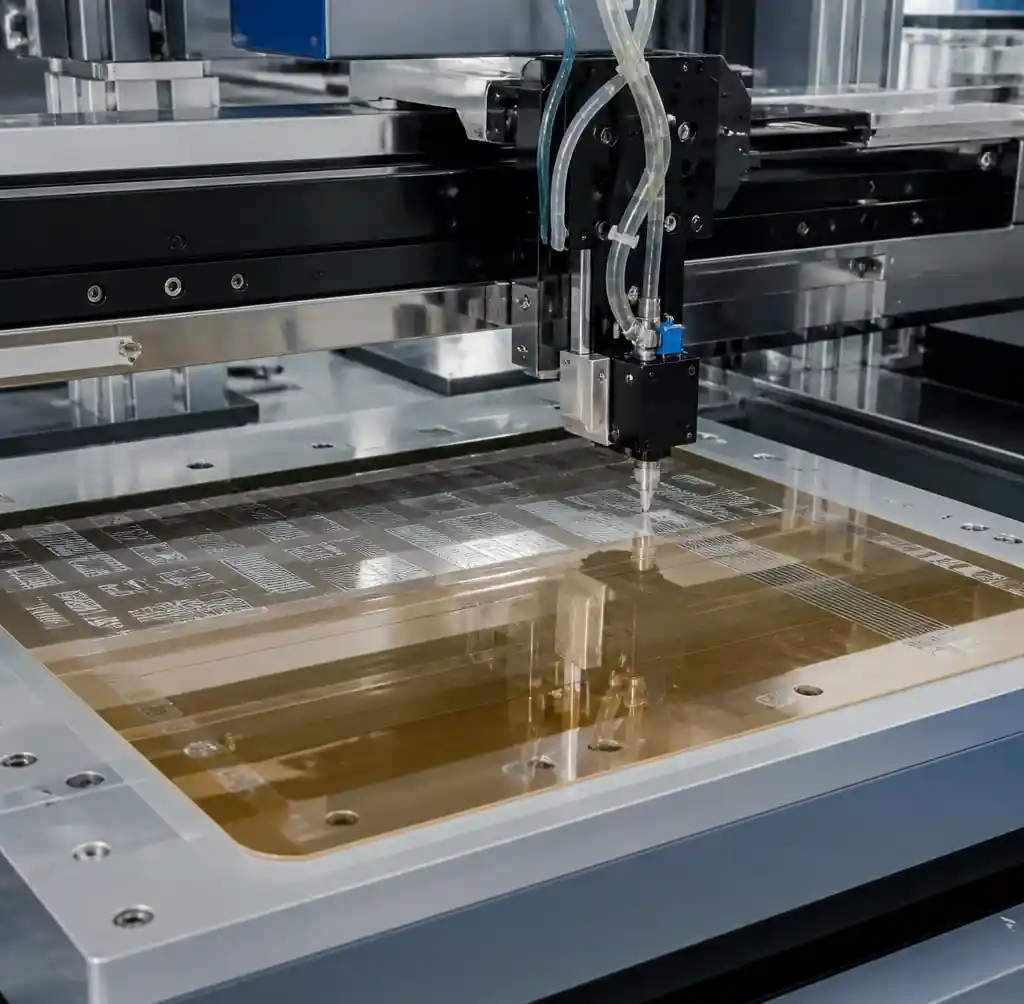
FHE relies on three primary deposition methods. Screen printing deposits silver or carbon inks through a stencil mask, achieving 50–100 µm line widths for interconnects and electrodes. Inkjet printing jets functional inks onto substrates with 20–50 µm resolution, enabling direct patterning of sensors, resistors, and capacitors without masks. Aerosol jet printing uses focused aerosol streams to print 10 µm features on non-planar surfaces, critical for conformal antennas and strain gauges.
Each process trades resolution for throughput. Screen printing handles high-volume production but cannot match inkjet’s design flexibility. Aerosol jet reaches the finest features but runs slower than screen methods. Production lines often combine all three, printing coarse power traces via screen, fine sensor patterns via inkjet, and conformal features via aerosol jet.
Component Integration Methods
After printing passive structures, FHE assembly integrates active silicon devices. Chip-on-flex (COF) bonds bare die directly to printed substrates using anisotropic conductive film (ACF) or non-conductive paste (NCP), eliminating package height and enabling ultra-thin profiles. Surface mount assembly places packaged components—QFN, BGA, or chip-scale packages—using standard pick-and-place equipment adapted for flexible handling.
The challenge is thermal mismatch. Silicon’s coefficient of thermal expansion (CTE) is 2.6 ppm/°C; polyimide ranges from 12–20 ppm/°C. Reflow soldering at 250°C induces stress that can crack solder joints or delaminate layers. FHE mitigates this through low-temperature sintering of printed silver inks (150–200°C), elastomeric underfills that absorb strain, and island designs that isolate rigid component zones from flex regions.
Encapsulation and Protection
Wearable and outdoor applications expose FHE to sweat, humidity, and mechanical abrasion. Parylene coating provides conformal protection down to 5 µm thickness with excellent moisture barrier properties (water vapor transmission rate <0.1 g/m²/day). Printed dielectric layers using UV-curable polymers seal interconnects while maintaining flexibility. Laminated coverlay films protect high-flex zones, similar to traditional flex PCB coverlay.
The tradeoff is breathability. Medical skin patches require moisture vapor transmission to prevent skin irritation, so fully sealed encapsulation is unacceptable. Designers use patterned coatings—sealing electronics while leaving vent paths—or breathable films like polyurethane that balance protection with comfort.
Key Application Areas
Wearable Health Monitoring
Medical-grade FHE patches integrate printed electrodes for biopotential sensing (ECG, EMG, EEG) with embedded microcontrollers and Bluetooth radios. The printed electrode array conforms to skin topology, reducing motion artifacts that plague rigid sensors. Abbott’s FreeStyle Libre glucose monitor and Medtronic’s continuous cardiac monitors exemplify commercial FHE deployment, with over 10 million units shipped as of 2026.
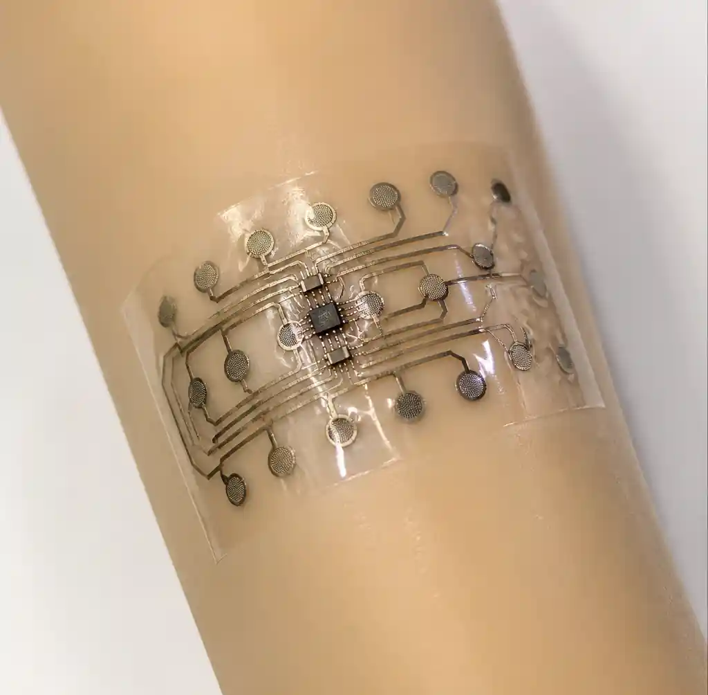
The performance requirement is 10,000+ bend cycles at 5 mm radius while maintaining electrode impedance below 100 kΩ at 10 Hz. Printed silver-chloride inks achieve this through stretchable binders that absorb strain. The accompanying silicon IC processes sensor data locally, transmitting only clinically relevant events to conserve battery life—a 1 mm² die running at 1 MHz draws under 10 µA, enabling 14-day operation from a printed zinc-air battery.
Smart Packaging and Supply Chain Tracking
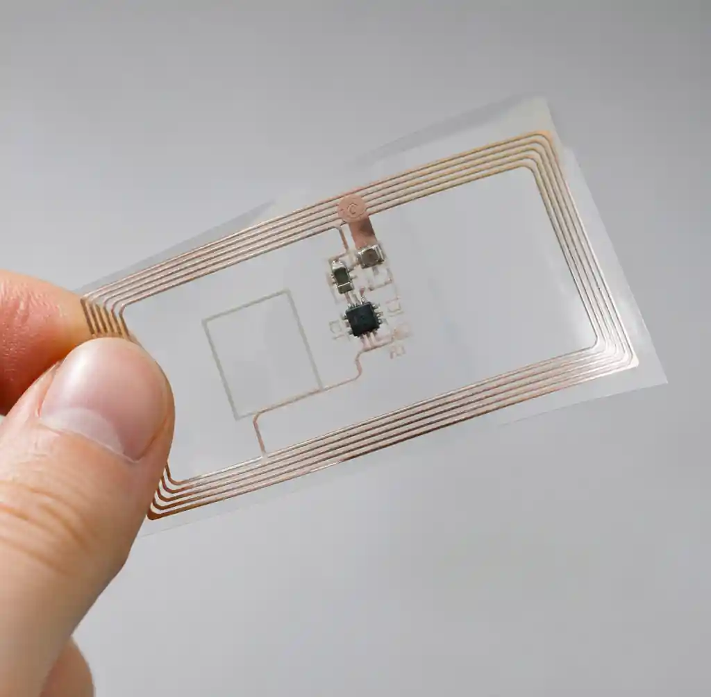
FHE enables “intelligent packaging” that monitors temperature, humidity, and shock during shipping. Thin-film sensors printed directly on cardboard detect cold chain breaks for pharmaceuticals or impact events for fragile electronics. The entire circuit—NFC antenna, temperature sensor, and memory chip—fits within a 0.2 mm profile, adding less than 1 gram per package.
Unlike RFID tags, FHE sensors actively log data throughout transit. A printed thermistor samples every 5 minutes; a 1 Mbit memory chip stores 30 days of readings. The NFC interface powers the circuit during scanning, eliminating batteries entirely. This architecture costs under $0.50 at volume, reaching the price point where single-use tracking becomes economically viable.
| Application | Key FHE Components | Form Factor | Typical Cost (Volume) |
|---|---|---|---|
| Glucose monitor patch | Printed enzyme electrode + MCU + BLE | 50 × 30 × 1 mm | $15–$25 |
| Cold chain sensor tag | Printed thermistor + NFC IC + memory | 80 × 50 × 0.2 mm | $0.30–$0.50 |
| Wearable ECG monitor | Printed Ag/AgCl electrodes + AFE IC | 100 × 60 × 2 mm | $8–$15 |
| Smart label (retail) | Printed antenna + E-ink display + MCU | 150 × 100 × 0.5 mm | $1–$3 |
IoT Sensor Networks
Structural health monitoring of bridges, aircraft, and industrial equipment demands hundreds of distributed sensors, each conforming to curved metal or composite surfaces. FHE strain gauges print directly onto structural members, measuring microstrain (±1,000 µε) with 0.1% accuracy. The printed sensor connects to a placed microcontroller that reports via low-power wide-area networks (LoRaWAN, NB-IoT).
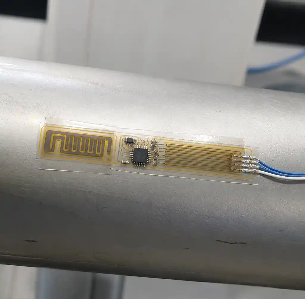
Traditional foil strain gauges require bonding adhesive, protective coating, and wired connections—installation labor exceeds $50 per sensor. Printed FHE gauges integrate sensing, processing, and wireless transmission in a single adhesive-backed patch, reducing installed cost to under $10. More importantly, the thin profile (0.3 mm) eliminates reinforcement effects that skew strain readings from thick bonded sensors.
Human-Machine Interfaces
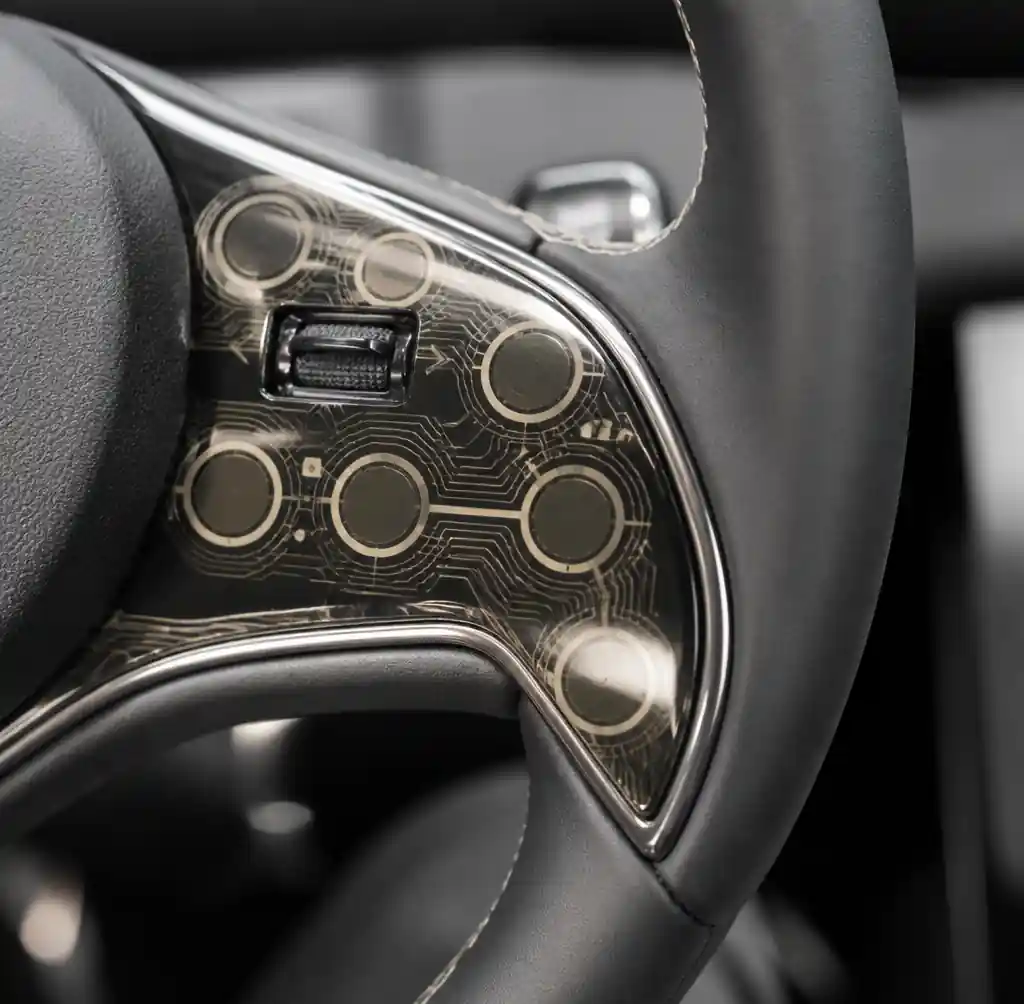
Automotive interiors increasingly replace mechanical switches with capacitive touch surfaces integrated into fabric, leather, and molded plastics. FHE touch sensors print conductive patterns directly onto non-planar 3D surfaces—steering wheel contours, door panels, armrests—that injection-molded rigid PCBs cannot follow.
The touch controller IC mounts in a low-stress zone (flat section of the dashboard), while printed silver traces route to sensor pads shaped to the molded surface. This distributed architecture keeps silicon in a mechanically stable region while placing sensing elements where human contact occurs. Automotive qualification (AEC-Q100) applies only to the rigid IC zone; the printed flex region follows durability testing per IPC-6013 with 100,000 touch cycles and -40°C to 85°C thermal cycling.
Design Guidelines for FHE
Material Selection
Substrate choice balances flexibility, thermal stability, and cost. Polyimide (Kapton, Upilex) handles reflow temperatures up to 260°C and survives 100,000+ bend cycles, but costs $50–$100/m² for 25 µm film. PET (polyethylene terephthalate) offers good flexibility at $5–$10/m² but degrades above 150°C, restricting assembly to low-temperature processes. PEN (polyethylene naphthalate) bridges the gap with 180°C thermal resistance at $15–$25/m².
Conductive ink selection determines long-term reliability. Silver flake inks achieve 3–5 µΩ·cm resistivity after sintering at 150°C, approaching bulk silver (1.6 µΩ·cm). Carbon inks reach 50–100 µΩ·cm but cost 70% less and survive higher strain before cracking. Stretchable silver inks with elastomeric binders maintain conductivity up to 30% elongation, critical for textile integration.
Mechanical Design Rules
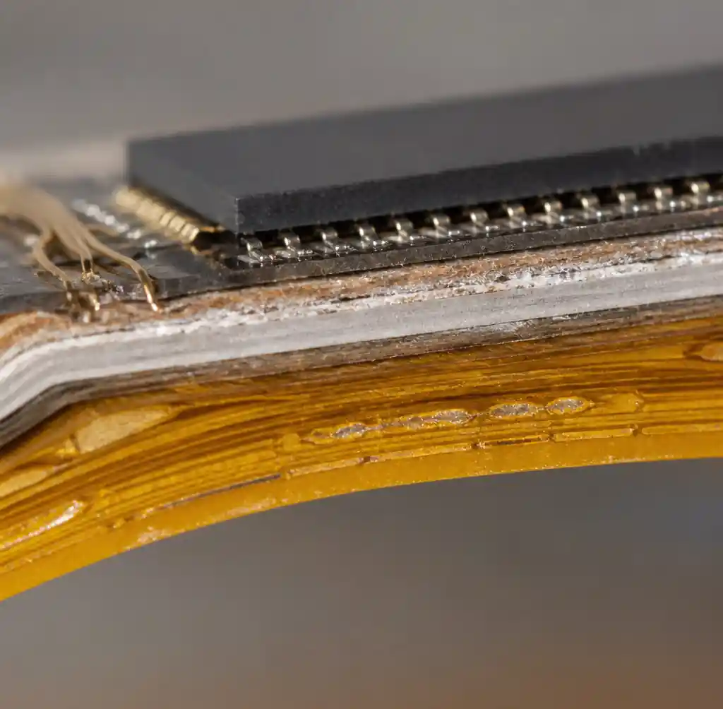
Rigid IC islands must isolate from high-strain zones. A 5 mm × 5 mm IC on a 50 µm substrate creates a stiffness discontinuity that concentrates stress at the island perimeter. IPC-2223 recommends transitioning from rigid to flex over a distance at least 3× the substrate thickness—for 100 µm material, that’s 0.3 mm minimum taper length. In practice, we use 1–2 mm transition zones with gradually reduced copper fill to smooth the stiffness gradient.
Trace routing through flex zones follows controlled impedance design principles. Differential pairs for USB or MIPI signals must maintain consistent spacing, but flexing changes dielectric thickness. FHE compensates by printing thicker dielectric layers (30–50 µm vs. 12 µm prepreg in traditional flex) and widening traces by 10–15% in dynamic bend regions to maintain 100Ω ±10% impedance.
Thermal Management
Printed interconnects dissipate heat poorly compared to etched copper. A 100 µm wide, 5 µm thick printed silver trace has 5× the resistance of equivalent 18 µm electrodeposited copper. At 500 mA current, the printed trace generates 0.15 W/cm, raising local temperature by 20–30°C without thermal relief.
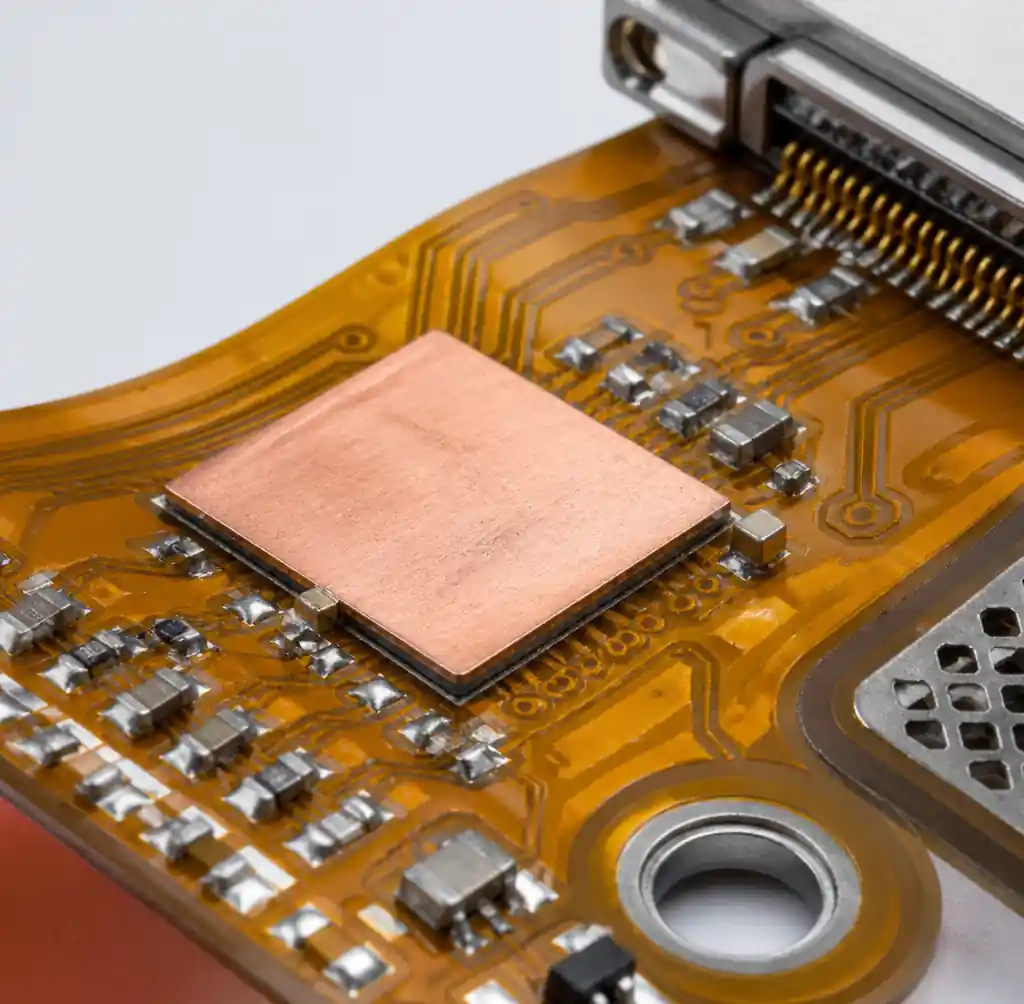
FHE addresses this through hierarchical thermal design. High-current paths (battery feeds, motor drivers) use screen-printed silver traces 200–500 µm wide with 10–15 µm thickness, achieving <10 mΩ/cm resistance. Low-current signal traces use inkjet-printed features as narrow as 50 µm. Power ICs mount on small copper heat spreaders (0.1 mm copper sheet embedded in the flex stack), connected to the rigid component island to sink heat away from the thin flex region.
Cost Considerations
FHE manufacturing involves capital-intensive printing equipment and lower material utilization than traditional PCBs. A production-scale screen printer costs $150k–$300k; aerosol jet systems run $400k–$800k. Material waste is higher because printed inks cannot be reclaimed like etched copper, and rejected substrates represent sunk costs in deposited materials.
At volumes below 10,000 units, FHE costs 3–5× more than equivalent rigid-flex PCB designs. The crossover occurs at 50,000–100,000 units, where amortized tooling and reduced assembly (fewer connectors, no cable harnesses) tip the economics in FHE’s favor. For applications requiring millions of units—consumer wearables, disposable medical sensors, smart packaging—FHE reaches cost parity with traditional manufacturing.
| Volume | FHE Cost per Unit | Rigid-Flex PCB Cost per Unit | Cost Ratio |
|---|---|---|---|
| 1,000 | $45–$80 | $15–$25 | 3–5× |
| 10,000 | $18–$35 | $8–$15 | 2–3× |
| 100,000 | $6–$12 | $5–$10 | 1.2–1.5× |
| 1,000,000+ | $2–$5 | $3–$7 | 0.7–1.2× |
The hidden cost advantage is assembly elimination. A rigid PCB connected to sensors via FPC cables requires connector soldering, cable routing, and mechanical strain relief—labor that adds $2–$5 per unit. FHE integrates sensors directly, removing these assembly steps. For wearables, this labor savings offsets the higher substrate cost even at moderate volumes.
Market Trends and Industry Adoption
The global FHE market reached $271.68 million in 2026 and projects to $1,287.45 million by 2035, growing at 16.86% CAGR according to market research data. Wearable health devices drive 45% of demand, followed by IoT sensors (28%) and smart packaging (18%). NextFlex, the U.S. manufacturing institute for FHE, reports over 120 member organizations actively developing FHE products as of 2026.
Automotive adoption accelerates as OEMs replace mechanical controls with conformal touch surfaces. General Motors’ 2026 model year integrates FHE touch panels in 8 vehicle lines; Ford projects 40% of interior switches will transition to FHE by 2028. The reliability requirement is 15 years and 300,000 touch actuations per IPC-9252 automotive test standards—validation that took three years of accelerated lifecycle testing to prove.
Medical device makers face longer approval cycles but higher margins. FDA 510(k) clearance for wearable glucose monitors requires clinical validation showing accuracy within ±15% of laboratory reference. Abbott’s continuous glucose monitor, using FHE with printed enzyme electrodes, achieved this specification with 95% of readings in the acceptable range across a 10,000-patient trial. The device now captures 60% of the U.S. continuous glucose monitoring market.
Integration with Andwin Circuits’ Capabilities
As a manufacturer specializing in HDI multilayer PCB and rigid-flex solutions, Andwin Circuits supports FHE development through hybrid substrate fabrication. Our process combines traditional flex circuit etching for high-density interconnects (50 µm line/space) with reserved zones for customer-applied printed electronics. This “prepared substrate” approach lets designers pattern sensors and passive components using their own printing equipment while relying on proven copper circuitry for power and high-speed signals.
For prototyping, we offer quick-turn PCB assembly with 3–5 day turnaround on flex and rigid-flex substrates optimized for subsequent printing. The stackup includes polyimide base layers treated for ink adhesion, strategically placed copper islands for component mounting, and controlled impedance routing that maintains electrical integrity after printing additional dielectric layers. This hybrid manufacturing model reduces FHE development risk by decoupling the high-yield copper circuit from experimental printed elements.
Testing and Reliability
FHE reliability testing combines flex PCB standards (IPC-6013) with printed electronics durability protocols. Bend cycle testing subjects the assembly to 10,000–1,000,000 flexes at specified radius, monitoring electrical continuity and resistance change. Acceptance criteria: <5% resistance increase for interconnects, <10% for printed sensors. Peel strength testing measures adhesion between printed layers and substrate, requiring >1 N/mm for medical-grade applications.
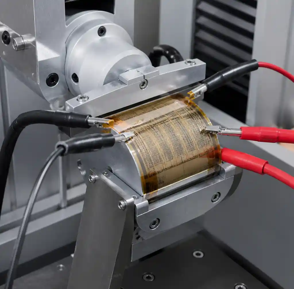
Environmental testing follows modified IPC-TM-650 methods. Temperature cycling (-40°C to 85°C, 500 cycles) validates CTE mismatch tolerance between silicon ICs and printed substrates. Humidity aging (85°C/85% RH, 1,000 hours) checks moisture barrier integrity of encapsulation layers. Mechanical abrasion (Taber test, 1,000 cycles) ensures wearable surfaces survive textile contact.
Accelerated testing predicts field life. A wearable device flexing 50 times per day for 2 years requires 36,500 cycles minimum. Safety margin pushes testing to 100,000+ cycles. A printed interconnect surviving this test demonstrates reliability margins sufficient for medical-grade wearables. Automotive applications demand 300,000 cycles at -40°C and +85°C extremes—qualification that only a few FHE manufacturers have demonstrated as of 2026.
FAQs
What is the main difference between FHE and traditional flex PCB?
FHE uses printed (additive) electronics for interconnects and sensors combined with placed silicon ICs, while traditional flex PCB etches (subtractive) copper traces on polyimide. FHE achieves thinner profiles (<100 µm), greater stretchability (>20% strain), and lower tooling costs for simple designs, but traditional flex PCB delivers higher conductor density and better high-frequency performance for complex multilayer routing.
Can FHE replace rigid-flex PCB in wearable devices?
For many wearables, yes. FHE suits applications where sensors and electronics integrate into a single conformal structure—health patches, smart textiles, flexible displays. However, rigid-flex PCB remains necessary when dense component population (BGA packages, high pin-count connectors) or high-speed protocols (PCIe, HDMI) are required, because printed interconnects cannot match the density or impedance control of etched copper.
What are typical lead times for FHE prototype manufacturing?
FHE prototyping depends on printing infrastructure. Facilities with in-house screen and inkjet printing turn prototypes in 5–10 days. If printing is outsourced to specialty vendors, lead times extend to 3–4 weeks. Design iteration is faster than traditional PCB because changing printed patterns requires only new stencils or digital print files, not new photomask sets. High-volume production lead times match traditional flex PCB at 4–6 weeks.
How does FHE perform in high-temperature environments?
Substrate temperature limits govern FHE survivability. Polyimide-based FHE operates continuously at 150°C and tolerates short excursions to 200°C. PET substrates fail above 120°C. Printed silver inks maintain conductivity to 200°C but may migrate under bias at elevated temperature and humidity. For true high-temperature applications (>200°C sustained), metal core PCB or ceramic substrates remain necessary; FHE targets room-temperature to 85°C operating ranges typical of wearables and consumer IoT.
Is FHE compatible with standard PCB assembly equipment?
Partially. Pick-and-place machines, reflow ovens, and AOI systems handle FHE substrates if properly fixtured to prevent warping during heating. The challenge is substrate handling—thin flexible films require vacuum hold-down or support carriers. Many contract manufacturers adapted PCBA assembly lines by adding flex-specific fixtures and lower-temperature reflow profiles (peak 220–240°C vs. 260°C for rigid boards). Screen and inkjet printing require dedicated equipment that standard PCB assembly houses typically do not own.
What design files are needed for FHE manufacturing?
FHE requires two file sets: standard Gerber/ODB++ for etched copper layers and component placement, plus vector artwork (PDF, DXF, or printer-specific formats) for printed features. The printed artwork specifies ink type, layer thickness, and cure conditions. Designers also submit a stackup cross-section showing printed layer positions relative to copper layers, plus assembly drawings indicating which components mount before vs. after printing. This dual-format documentation reflects the hybrid manufacturing process.
Conclusion
Flexible hybrid electronics merges the scalability of printed manufacturing with the performance of silicon ICs, creating circuits that bend, stretch, and conform while retaining computational capability. The technology has moved from research labs to commercial production, with wearable health monitors and smart packaging representing the largest volume applications in 2026.
FHE suits designs where conformability drives system value—wearables that must follow body contours, sensors embedded in curved structures, and disposable electronics where cost-per-unit governs viability. It does not replace traditional PCBs or even flex circuits in most applications; rather, it opens design space that neither technology could address alone. The economic crossover occurs at 50,000–100,000 units, where printing’s lower tooling cost and reduced assembly offsets higher material expense.
For engineers evaluating FHE, the decision hinges on form factor constraints and production volume. If your product must flex dynamically, conform to complex 3D shapes, or integrate sensors directly into the substrate, FHE provides capabilities no other technology delivers. If your design fits on a flat or gently curved surface and volumes stay below 10,000 units, rigid-flex PCB remains more cost-effective. The future trajectory is clear: as printing equipment costs decline and material performance improves, FHE will expand into applications still dominated by conventional PCBs. That migration has already begun.